Concept of Ideal Operational Amplifiers
An ideal operational amplifier (op-amp) is a theoretical device used to simplify the analysis and design of electronic circuits.
An operational amplifier (op-amp) is defined as a direct current-coupled voltage amplifier that increases the input voltage passing through it. Ideally, an op-amp should have high input resistance, low output resistance, and very high open-loop gain. In an ideal op-amp, the input resistance and open-loop gain are infinite, while the output resistance is zero.
An ideal op-amp has the following characteristics—
| Characteristic | Value |
|---|---|
| Open-Loop Gain (A) | ∞ |
| Input Resistance | ∞ |
| Output Resistance | 0 |
| Bandwidth of Operation | ∞ |
| Offset Voltage | 0 |
An ideal op-amp is defined as a differential amplifier with infinite open-loop gain, infinite input resistance, and zero output resistance. The ideal op-amp has zero input current because its infinite input resistance creates an open circuit at the input. This means there is no current at either input terminal.
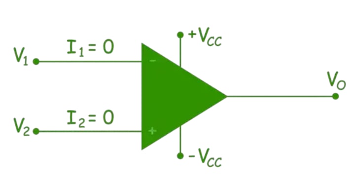
With no current through the input resistance, there is no voltage drop between the input terminals. Thus, no offset voltage appears across the inputs of an ideal operational amplifier.
If and are the voltages at the inverting and non-inverting terminals of the op-amp, and , then in an ideal case:
The bandwidth of operation of an ideal op-amp is also infinite. This means the op-amp performs its function across all ranges of operating frequencies.
Negative Feedback in Operational Amplifier (Op-Amp) Circuits
In an op-amp circuit with negative feedback, a portion of the output signal is fed back to the inverting input of the op-amp. This feedback reduces the overall gain but significantly enhances the stability, linearity, and accuracy of the amplifier circuit.
When negative feedback is applied, the op-amp adjusts its output to maintain the input difference (between the non-inverting and inverting terminals) close to zero. This behavior is known as the virtual short or virtual ground principle, and it is a key characteristic of op-amps with negative feedback.
How Negative Feedback Works:
In a typical op-amp circuit:
- The non-inverting input receives the input signal.
- The inverting input receives a portion of the output signal as feedback.
If the output voltage deviates due to changes in the input or other factors, the negative feedback signal corrects this deviation by driving the inverting input. This causes the op-amp to stabilize the output. This self-correcting mechanism reduces errors and keeps the amplifier's output stable and proportional to the input.
Benefits of Negative Feedback in Op-Amps
-
Improves Linearity and Reduces Distortion:
- Negative feedback minimizes nonlinear distortion by reducing the gain of the op-amp, making the output signal more accurately proportional to the input signal.
- By correcting deviations from the ideal linear output, negative feedback suppresses harmonic distortion, which is often introduced by imperfections in the active components.
- This makes the amplifier suitable for applications requiring high fidelity, such as audio amplifiers, where even small distortions in sound can be noticeable.
-
Stabilizes Gain:
- In an open-loop (no feedback) configuration, op-amps have extremely high gain (often in the range of tens or hundreds of thousands). This high gain is sensitive to temperature, power supply variations, and component tolerances.
- Negative feedback reduces this gain to a predictable, stable, and lower value, which depends only on the external feedback network (e.g., resistors or other components used in the feedback path). This makes the amplifier's gain independent of the op-amp's intrinsic characteristics.
-
Increases Bandwidth:
- Without feedback, op-amps have limited bandwidth, with gain dropping as frequency increases.
- Negative feedback extends the bandwidth by allowing higher frequencies to pass through with less attenuation. In fact, the gain-bandwidth product (GBW) of the op-amp typically remains constant, meaning that as the gain is reduced by feedback, the bandwidth increases.
- This makes the amplifier suitable for high-frequency applications, such as video amplifiers and signal conditioning circuits.
-
Reduces Noise Sensitivity:
- Noise in amplifiers can originate from many sources, including temperature fluctuations, power supply instability, and component imperfections.
- Negative feedback helps suppress noise by minimizing the difference between the op-amp’s inputs, thereby reducing the amount of noise amplified along with the signal.
- This results in a cleaner output signal and makes the circuit more robust to external noise, especially in low-level signal applications.
-
Improves Input and Output Impedance:
- Negative feedback increases the input impedance and decreases the output impedance of the amplifier.
- High input impedance ensures that the amplifier does not load the source, preserving the original signal.
- Low output impedance enables the amplifier to drive loads more effectively without significant voltage drop, making it ideal for interfacing with other stages in a signal chain.
- These improvements in impedance matching are crucial for ensuring minimal signal loss and efficient energy transfer between stages.
-
Thermal Stability:
- Op-amp circuits can be sensitive to temperature changes, which affect the behavior of internal transistors and other components.
- Negative feedback reduces the impact of temperature variations by stabilizing the operating point of the circuit.
- This results in thermal stability, ensuring that the amplifier maintains consistent performance across different operating conditions.
Ideal Operational Amplifier Parameters
The ideal operational amplifier (op-amp) has several theoretical parameters that define its behavior. These parameters simplify circuit analysis and design, even though they can't be fully realized in practical op-amps.
- Output Offset Voltage
- Input Offset Voltage
- Input Offset Current
- Input Bias Current
- Common-Mode Gain
- Common-Mode Rejection Ratio
- Supply Voltage Rejection Ratio
- Thermal Drift
- Slew Rate
1. Output Offset Voltage:
The voltage present at the output without any input applied is called output offset voltage. It occurs due to the two differential amplifier stages in the op-amp. The output offset voltage in an operational amplifier (op-amp) is the unwanted DC voltage that appears at the output when the input is ideally zero (i.e., both input terminals are at the same voltage). This offset voltage results from imperfections in the op-amp.
2. Input Offset Voltage:
When the non-inverting and inverting inputs are grounded, ideally, the output should be zero. However, due to the two stages of differential amplifiers, a small output voltage appears. To nullify this output voltage, some voltage is required to be applied to either of the two inputs. This is called the input offset voltage.
3. Input Offset Current ():
Input offset current is a parameter of operational amplifiers (op-amps) that refers to the difference between the DC bias currents entering the inverting and non-inverting input terminals of the op-amp. Ideally, these input currents should be identical, but due to internal mismatches in the op-amp, there is often a small difference between them.
4. Input Bias Current ():
It is the average of the currents that flow into the inverting and non-inverting terminals of the operational amplifier. The input bias current is the average of the currents flowing into the inverting () and non-inverting () input terminals of the op-amp:
This current is necessary for the proper functioning of the op-amp.
5. Common-Mode Gain:
When the same input voltage is applied to both input terminals of an op-amp, the op-amp is said to be operating in a common-mode configuration. Common-mode gain () is the gain applied to signals that are present on both input terminals of the op-amp. Ideally, an op-amp should have zero common-mode gain, meaning it should not amplify common-mode signals at all.
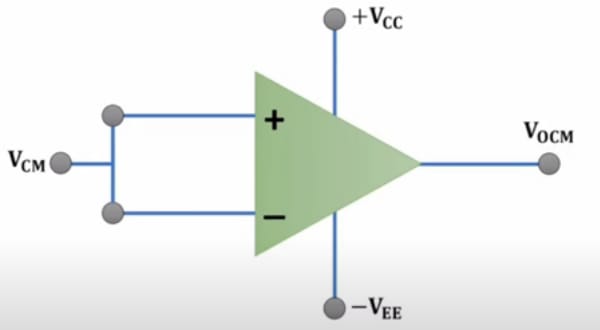
Common-mode gain () =
6. Common-Mode Rejection Ratio (CMRR):
It is the ratio of the differential gain and common-mode gain.
Also,
7. Supply Voltage Rejection Ratio (SVRR):
SVRR is the change in an op-amp's input offset voltage () caused by variations in supply voltages.
Manufacturers also use terms like PSRR (Power Supply Rejection Ratio) and PSS (Power Supply Sensitivity). PSRR indicates how well the op-amp rejects variations in its power supply voltage. An infinite PSRR implies that changes in the power supply have no effect on the output voltage.
8. Thermal Drift:
Ideally, parameters of an op-amp like , , and remain constant, but practically, they change with temperature, supply, and time. The average rate of change of input offset voltage per unit change in temperature is called thermal voltage drift.
Thermal Voltage Drift =
Thermal Current Drift =
Thermal Drift in Input Bias Current =
9. Slew Rate:
Slew rate is defined as the maximum rate of change of output voltage per unit time. It is expressed in terms of volts per microsecond.
Slew Rate =
Inverting Amplifiers
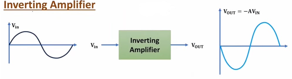
An inverting operational amplifier is a device used in electronics engineering for amplifying signals and generating an output voltage that is 180° out of phase with the input waveform. It typically consists of an operational amplifier and some resistors.
The inverting operational amplifier can be described as an amplifier with fixed gain, which produces a negative output voltage because its gain is always negative.
We can say that the output of an inverting operational amplifier is out of phase with its input by 180°. This means that for a negative input pulse, the output will be positive, and for a positive input pulse, the output will be negative.
Working of the Operational Amplifier:
-
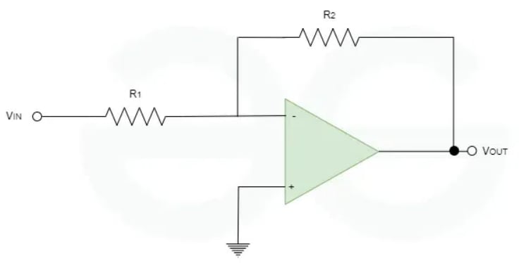
The inverting terminal of the inverting operational amplifier is fed with the input signal, while the non-inverting terminal is usually connected to ground or some reference voltage.
-
Next, a feedback circuit is applied. In this configuration, a feedback resistor is connected between the output of the op-amp and the inverting input terminal. This resistor primarily controls the gain.
-
An ideal op-amp amplifies the input voltage applied. The negative feedback from the output to the inverting input creates a stable condition, helping to control the output generated. The op-amp works to ensure that the voltage at the inverting input equals the voltage at the non-inverting input.
-
Due to the inverting nature, the input signal is inverted. This means that if the input signal increases, the output will decrease, and vice versa. The gain of the final output is calculated using the formula .
-
After amplification and inversion of the input signal along with phase inversion, the output wave is generated at the junction. The output voltage is denoted by .
Inverting Amplifier Equation and Gain:
Let's derive the gain of an op-amp.
Mathematically, the voltage gain can be written as:
Where,
and
An ideal op-amp has infinite input impedance, meaning the currents flowing into its input terminals are zero.
Thus, . We also know that in an ideal op-amp, the voltage at the inverting and non-inverting inputs is always equal. Hence,
Due to virtual ground, .
Also,
.
So,
and
We combine the last two equations:
so,
This is how we derive the gain of an inverting operational amplifier.
Advantages of Inverting Operational Amplifier:
There are various advantages of an inverting operational amplifier, some of which are listed below:
-
The configuration of an inverting operational amplifier makes it more stable compared to a non-inverting operational amplifier. The stability and predictability of these op-amps make them easier to analyze.
-
The output gain of an inverting operational amplifier depends on the resistances used, so by selecting appropriate resistance values, we can achieve high gains with large amplifications of input waveforms.
-
The non-inverting input of this operational amplifier is grounded, so the inverting input acts as a virtual ground. This simplifies circuit design and analysis.
-
One important advantage of an inverting operational amplifier is its ability to phase-invert. This helps to produce an output that is out of phase with the input wave by 180°. Thus, it can be used in phase-shift circuits.
-
Inverting operational amplifiers have high input impedance and low output impedance. The high input impedance helps to drain very little current from the input waveform, and the low output impedance helps to carry low-input impedance loads without signal loss.
Disadvantages of Inverting Operational Amplifier:
There are certain disadvantages of inverting operational amplifiers, some of which are listed below:
-
Due to its configuration, an inverting operational amplifier often exhibits more noise compared to a non-inverting operational amplifier. This noise can be an important consideration when designing circuits.
-
Designing circuits with inverting operational amplifiers can be a complicated procedure. Sometimes, achieving a specific gain requires complex feedback circuits. This can increase the number of components and the cost.
-
Inverting operational amplifiers are not suitable when precise output is required. This is because they are sensitive to input offset voltage, which can lead to errors in the final output.
-
Inverting operational amplifiers have some limitations when used in common mode. The common mode limits the input range, and any voltage beyond or below this range will distort the output voltage.
-
Sometimes, the inversion provided by an inverting operational amplifier is undesirable. This can cause unnecessary phase shifting, and extra circuits might be needed for correction.
Non-Inverting Amplifiers
A non-inverting amplifier is an op-amp that outputs a signal with the same polarity as the input, ensuring the gain is always positive.
A non-inverting amplifier is defined as an operational amplifier that amplifies input signals without reversing their polarity, resulting in a positive voltage gain. A non-inverting operational amplifier or non-inverting op-amp uses an op-amp as the main element. An op-amp features two input terminals: the inverting input marked with a minus sign (-) and the non-inverting input marked with a plus sign (+).
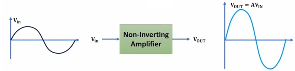
Applying a signal to the non-inverting input results in an amplified output that retains the original signal's polarity. Consequently, the gain from a non-inverting amplifier configuration is always positive.
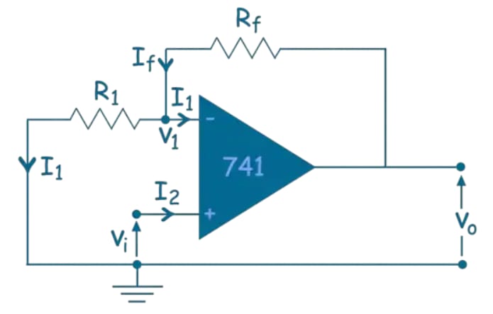
In the above circuit, we connect an external resistance and feedback resistance at the inverting input. Now, by applying Kirchhoff's Current Law, we get:
Let us assume the input voltage applied to the non-inverting terminal is .
Now, if we assume that the op-amp in the circuit is an ideal op-amp, then:
Therefore, equation (i) can be rewritten as:
The closed-loop gain of the circuit is:
This term does not contain any negative parts. Hence, it proves that the input signal to the circuit gets amplified without changing its polarity at the output.
From the expression of the voltage gain of a non-inverting op-amp, it is clear that the gain will be unity when or .
When ,
When ,
So, if we short circuit the feedback path and/or open the external resistance of the inverting pin, the gain of the circuit becomes 1.
Non-Inverting Amplifier Equation:
Advantages of Non-Inverting Amplifier:
-
Positive Gain: Non-inverting amplifiers provide a positive gain, which means the output voltage is in phase with the input voltage. This is advantageous in applications where the signal polarity needs to be preserved.
-
High Input Impedance: Non-inverting amplifiers typically have a very high input impedance. This means they do not load the input source significantly, allowing for accurate signal amplification without affecting the original signal.
-
Stability: The feedback configuration of non-inverting amplifiers contributes to their stability. They are less prone to oscillations and are generally more stable than inverting amplifiers.
-
Signal Integrity: Non-inverting amplifiers maintain the integrity of the input signal by preserving its polarity. This is especially useful in situations where the phase of the signal is crucial.
Disadvantages of Non-Inverting Amplifier:
-
Limited Gain Control: While non-inverting amplifiers provide positive gain, the gain control is more limited compared to inverting amplifiers. Achieving high gains may require larger resistor values, which can affect the circuit's performance.
-
Lower Precision: Non-inverting amplifiers may have slightly lower precision compared to inverting amplifiers, especially in applications where precise gain control is essential.
-
More Complex Circuit: The design of non-inverting amplifiers can be slightly more complex than inverting amplifiers, requiring careful selection of components to achieve the desired gain and stability.
-
Phase Shift: While non-inverting amplifiers preserve the polarity of the input signal, they may introduce a slight phase shift, especially at higher frequencies. This can be a disadvantage in certain applications.
Difference Between Inverting and Non-Inverting Op-Amp:
| Inverting Op-Amp | Non-Inverting Op-Amp |
|---|---|
| The type of feedback used is voltage shunt. | The type of feedback used is voltage series. |
| Gain formula: | Gain formula: |
| Output is 180° out of phase with the input signal. | Output is in-phase with the input. |
| The gain can be less than, equal to, or greater than 1. | The gain is always greater than 1. |
| Output voltage is high for less than . | Output voltage is high for greater than . |
| Input is applied to the inverting terminal of the op-amp. | Input is applied to the non-inverting terminal of the op-amp. |
| The input impedance is . | The input impedance is very high. |
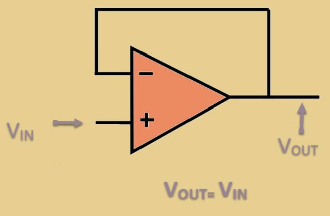
Unity Gain Amplifier
A Unity Gain Amplifier, also known as a Voltage Follower or Buffer Amplifier, is a type of operational amplifier (op-amp) configuration where the output voltage is exactly the same as the input voltage. In this configuration, the gain of the amplifier is 1 (or unity), hence the name "unity gain."
-
A unity gain amplifier is typically implemented using a non-inverting op-amp configuration with a feedback loop directly connecting the output to the inverting input.
-
The non-inverting input receives the input signal, while the inverting input is connected to the output through a direct wire or a resistor (with the same value as the input resistor).
-
The op-amp adjusts the output voltage so that the voltage difference between its inverting and non-inverting inputs is zero. In this case, because the output is fed back directly to the inverting input, the output voltage is forced to follow the input voltage exactly.
The gain of a unity gain amplifier is 1, meaning:
-
A unity gain amplifier has a very high input impedance, which means it does not load the previous stage of the circuit. This is beneficial in applications where the signal source has high impedance.
-
The output impedance is very low, making the amplifier capable of driving low-impedance loads effectively.
Advantages of Unity Gain Amplifier:
-
High Input Impedance: A unity gain amplifier presents a very high input impedance, which means it does not draw significant current from the input signal source.
-
Low Output Impedance: The low output impedance allows the amplifier to drive low-impedance loads effectively without significant signal loss. This makes it suitable for connecting to subsequent stages of a circuit that require a low-impedance input.
-
Minimal Signal Distortion: Since the gain is unity (1), the output is a faithful reproduction of the input signal with no amplification or attenuation, leading to minimal signal distortion.
-
Impedance Matching: Unity gain amplifiers are frequently used for impedance matching between high-impedance signal sources and low-impedance loads, ensuring maximum power transfer and signal integrity.
-
Level Shifting: They can be used for level shifting or interfacing between circuits operating at different voltage levels without altering the signal amplitude.
Disadvantages of Unity Gain Amplifier:
-
No Voltage Gain: The main limitation of a unity gain amplifier is that it provides no voltage gain. It can only buffer the signal and does not amplify it. If amplification is needed, a different configuration must be used.
-
Noise Introduction: Even though the gain is unity, the op-amp can introduce noise into the signal. This noise may become significant in low-level signal applications, where signal integrity is critical.
-
Limited Current Drive: While unity gain amplifiers have low output impedance, they may still have limitations in terms of the maximum current they can supply to the load.
-
Slew Rate Limitation: The slew rate of the op-amp can limit the performance of a unity gain amplifier, particularly in high-speed or high-frequency applications.
-
Bandwidth Limitation: Although unity gain amplifiers generally have a wide bandwidth, their bandwidth is not infinite. High-frequency signals may still experience attenuation or phase shift, depending on the op-amp's characteristics.
Adder or Summing Amplifier
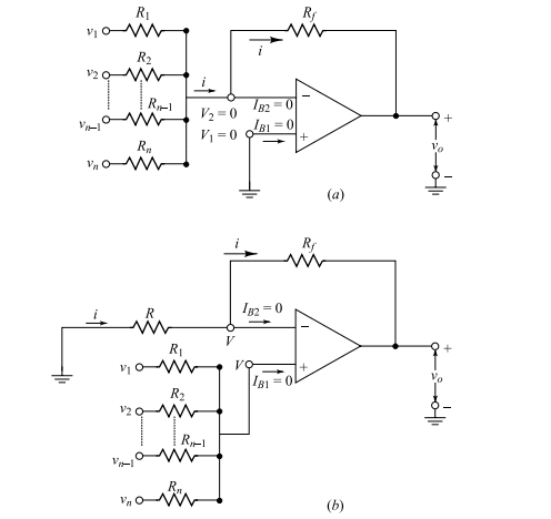
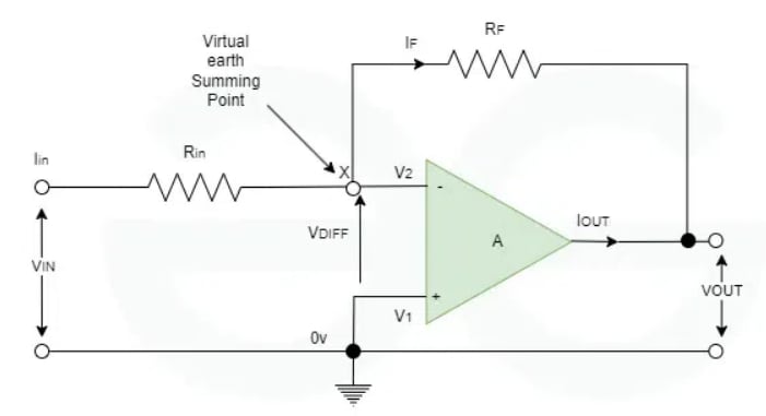
The circuit shown in Fig(a) is used to obtain an output that is a linear combination of multiple input signals. Applying the virtual ground concept, we can write:
which simplifies to:
For , we get:
In this case, the output is the sum of the inverted inputs. In the more general case of Eq. (i), the scale of each input signal may be adjusted before summing. Such an adder circuit is known as an inverting adder or summing amplifier.
To express , the output of Fig(a) must be applied as the input to an inverting amplifier with unity gain, requiring an additional amplifier.
Fig(b) shows a non-inverting adder circuit where the output can be directly expressed as the summation of inputs . Here, the input voltages are connected to the non-inverting terminal through resistances .
Let be the voltage at the non-inverting terminal. Since the op-amp draws no current, we have:
This gives:
Note that the circuit in Fig(b) can be considered as a non-inverting amplifier with input voltage . Thus, using the gain equation:
The output voltage can be written as:
For , Eq. (iv) simplifies to:
In general, Eq. (iv) shows that the output can be expressed as a linear combination of the inputs .
Subtractor
The following figure shows an op-amp circuit where the output voltage is expressed in terms of the input voltages and as or where and are arbitrary constants.
To understand the operation of the circuit, consider that the voltage at the non-inverting input terminal is . Since the same current flows through and , we have:
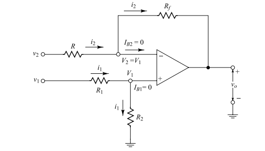
Since the voltage at the inverting input terminal is , we obtain:
This gives:
where:
For , Eq. (viii) results in , and thus the circuit acts as a simple subtractor with output voltage:
Integrator
The following figure shows an op-amp circuit where the output voltage is proportional to the integration of the input voltage . The output can be determined as follows.
For an ideal op-amp, we can write:
which simplifies to:
where we have used as the instantaneous charge of the capacitor and as the initial charge of the capacitor.
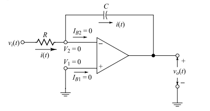
If the input voltage is constant, , then the output will be a ramp:
This type of integrator, known as a Miller integrator or Miller sweep, is excellent for generating sweep signals in a cathode-ray-tube oscilloscope.
If the input signal is a square wave, Eq. (xi) indicates that the output waveform of the integrator will be a triangular wave. Thus, an integrator can be used as a wave-shaping circuit.
Note that if we replace by a capacitor in the adder circuit of Fig(a), the circuit will simultaneously integrate and add. In this case, we can write:
which simplifies to:
Differentiator
Interchanging the position of the capacitor C and resistor R in Fig. of Intergrator, we can get a differentiator circuit where the output is proportional to the derivative of . Figure shows the schematic diagram of a differentiator circuit using an op-amp. In this case
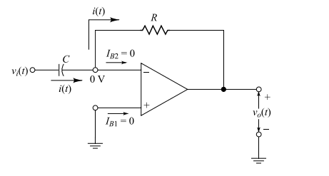
which gives the output voltage as
It may be mentioned that if the input is a triangular waveform, the output voltage waveform of will be a square wave. Thus a differentiator circuit can be used as a wave shaping circuit.
Logarithmic Amplifier
A basic logarithmic amplifier, or log-amp, circuit is shown in the figure below. As its name implies, this circuit produces an output voltage that is a logarithmic function of the input voltage . The analysis of this circuit proceeds as follows.
The virtual ground concept of an ideal op-amp suggests that the voltage at the inverting terminal, as well as at the collector of the BJT, is zero. The collector current must therefore equal the current flowing through the resistor .
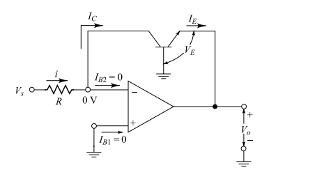
Since the collector potential is zero and the base is grounded, the transistor behaves like a p-n junction diode formed between the base (p) and emitter (n) regions of the transistor. Using the equation:
with , the emitter current of the BJT can be expressed as:
where is the reverse saturation current of the base-emitter junction, and:
is the thermal voltage, and is the forward bias voltage between the base and emitter junction of the BJT.
Note that for a grounded base BJT. Using in Eq. (xiv), the output voltage can be given by:
If , Eq. (xv) can be approximated as:
Thus, the output of the amplifier is a logarithmic function of the input voltage.
Comparator
An op-amp can be used in an open-loop configuration to compare an input voltage applied at one input terminal with a known reference voltage applied at the other input terminal. Such a circuit is called a comparator, as shown in Fig(a).
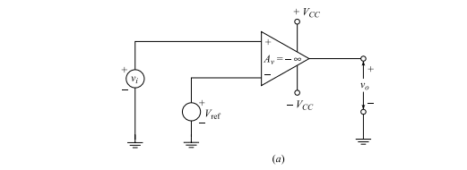
In this configuration, the input voltage and reference voltage are applied to the non-inverting and inverting input terminals, respectively. The output voltage is given by:
where is the open-loop gain of the op-amp, typically assumed to be very large (approaching infinity for an ideal op-amp). When are the biasing supply voltages, the maximum positive and maximum negative output voltage amplitudes are and , respectively, where is called the saturation voltage.
From Eq. (xvii), the output voltage of the comparator can be expressed as:
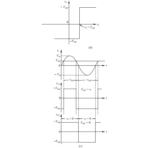
The transfer characteristic of the circuit is shown in Fig(b). The output voltages and corresponding to and , respectively, are demonstrated in Fig(c) for a sinusoidal input signal . Note that for , the output voltage changes its states where . Such a comparator circuit with zero reference voltage is known as a zero-crossing detector.
However, Eq. (xviii) is valid for all kinds of input and reference voltages in the circuit shown in Fig(a).