MOSFET
Metal-Oxide-Semiconductor Field-Effect Transistors (MOSFETs) are an advanced addition to the FET family, offering significant advantages in various applications. A MOSFET typically features a lightly doped P-type substrate with two heavily doped N-type regions diffused into it. One distinctive aspect of MOSFETs is their gate construction: the channel is completely insulated from the gate, which forms an electrostatic charge when voltage is applied.
The terminology used for MOSFET configurations reflects the FET electrode that is common to both the input and output circuits, leading to three main terms: common gate, common drain, and common source. Each configuration has specific characteristics:
-
Common Source:
This configuration is among the most widely used. It provides medium input and output impedance levels, with medium current and voltage gain. The output signal is inverted relative to the input (180° phase shift), making it popular for its balanced performance.
-
Common Drain:
Also known as the source follower, this configuration has the source voltage following the gate voltage. It offers high input impedance and low output impedance, making it ideal as a buffer.
-
Common Gate:
This configuration provides low input impedance and high output impedance. Although it has high voltage gain, the current gain and overall power gain are low compared to other FET configurations. It offers high isolation and feedback prevention, especially at high frequencies.
The gate region of a MOSFET is covered with metal, and the channel is insulated from the gate by a layer of silicon dioxide. This insulation is why MOSFETs are also called insulated gate FETs.
Working Principle of MOSFET
MOSFETs control conductivity based on the semiconductor channel between the drain and source terminals. This channel can be p-channel or n-channel depending on the MOSFET's configuration.
A MOSFET has three terminals: drain, source, and gate. Applying a voltage across the gate and source forms an inversion layer or channel between the drain and source if the voltage exceeds the threshold voltage. The threshold voltage is the minimum voltage required to induce conduction.
-
Cutoff Region (OFF): When the applied voltage is below the threshold, no channel forms, and current does not flow.
-
Saturation Region: Beyond a certain voltage, the current becomes constant. MOSFETs are voltage-controlled devices, so the channel thickness and current amount depend on the voltage applied across the gate and source. Increasing the gate voltage widens the channel, allowing more current to flow.
Types of MOSFETs
Depletion MOSFET
- Channels are present from the beginning, allowing current flow initially.
- Applying a negative voltage reduces the channel width and current flow.
- Less commonly used in modern devices.
Enhancement Mode MOSFET
- No channel is present initially, so no current flows at the start.
- Applying a positive voltage above the threshold voltage enhances the channel between the drain and source, increasing conductivity.
- Commonly used in digital applications.
Differences Between Enhancement and Depletion Type MOSFETs
| Enhancement Type MOSFET | Depletion Type MOSFET |
|---|---|
| By applying external voltage in the channel, if the amount of charge carriers increases, it is known as enhancement type MOSFET. | By applying external voltage in the channel, if the amount of charge carriers decreases, it is known as depletion type MOSFET. |
| No channel is present in the beginning. | Channel is present from the beginning. |
| There is a threshold voltage. | There is no such threshold voltage. |
| It does not produce current in the absence of . | It can produce current without any gate voltage. |
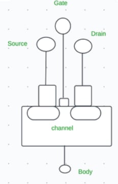
MOSFET Construction
MOSFETs (Metal-Oxide-Semiconductor Field-Effect Transistors) are widely used as switches, amplifiers, and in various other applications. The basic construction of a MOSFET includes the following components:
-
Substrate: The MOSFET is built on a silicon wafer, which serves as the base of the device.
-
SiO2 Layer: A thin layer of silicon dioxide (SiO2) is used as an insulating material between the gate and the semiconductor substrate, preventing direct current flow.
-
Gate Terminal: Positioned on the insulating layer, the gate terminal controls the flow of current between the drain and source by applying a gate voltage.
-
Source and Drain Terminals: These are doped regions created on either side of the gate. The source is where current enters the MOSFET, and the drain is where it exits.
-
Channel: The region between the gate, drain, and source. The channel controls the flow of charge carriers and is modulated by the gate voltage.
Working of N-Channel Enhancement Type MOSFET
For an N-channel enhancement-mode MOSFET:
-
Gate Voltage Application: A positive voltage is applied to the gate terminal. This positive voltage attracts electrons (negative charges) to the surface of the semiconductor substrate, forming an n-type channel.
-
Channel Formation: As the gate voltage increases, more electrons accumulate, creating a conductive channel between the drain and source.
-
Threshold Voltage: The voltage at which the channel forms is known as the threshold voltage. Once the gate voltage exceeds this threshold, current flows between the drain and source, and the channel width increases with higher gate voltage.

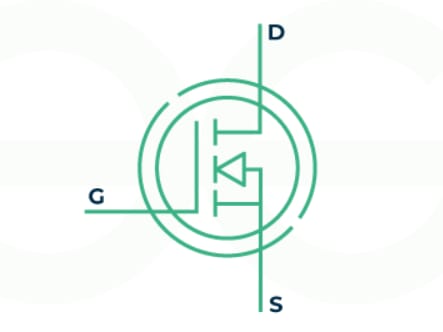
Symbol:

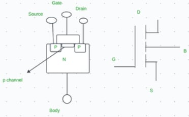
Working of P-Channel Enhancement Type MOSFET
For a P-channel enhancement-mode MOSFET:
-
Gate Voltage Application: A negative voltage is applied to the gate terminal. This negative voltage creates an electric field that attracts holes (positive charge carriers) to the surface, forming a p-type channel.
-
Channel Formation: When the gate voltage is sufficient, a conductive channel forms between the drain and source.
-
Current Flow: When the voltage is applied, holes move through the channel, allowing current to flow between the drain and source.

Symbol:

Working of N-Channel Depletion Type MOSFET
For an N-channel depletion-mode MOSFET:
-
Channel Presence: A channel is present from the beginning, so the MOSFET is generally on without applying any gate voltage.
-
Voltage Application: Applying a positive gate voltage creates a depletion region, which reduces the number of charge carriers and decreases current flow.
-
Control: The MOSFET can be turned off by applying a sufficient positive voltage, reducing current to a very low value or turning it off completely.

Symbol:

Working of P-Channel Depletion Type MOSFET
For a P-channel depletion-mode MOSFET:
-
Channel Presence: A channel is present from the start, allowing current to flow between the drain and source.
-
Voltage Application: Applying a negative gate voltage reduces the channel width by creating a depletion region, which decreases the current flow.
-
Control: The MOSFET acts as a voltage-controlled resistor, with current decreasing as the negative gate voltage increases.
Symbol:

Operating Regions of MOSFET
MOSFETs exhibit three main operating regions:
- Cut-Off Region: The MOSFET is OFF, with no conduction occurring. It behaves like an open switch.
- Ohmic Region: Current increases linearly with the voltage . In this region, MOSFETs operate as amplifiers.
- Saturation Region: The MOSFET is ON, with the current remaining constant despite increases in . This region is used for switching applications, where the device acts like a closed switch allowing a constant current flow.
Characteristics of MOSFET
MOSFETs have two primary characteristics:
- Drain Characteristics
- Transfer Characteristics
Enhancement Type MOSFET
1. Drain Characteristics of Enhancement Type MOSFET:
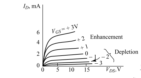
Drain characteristics describe the relationship between the output current () and the output voltage (Drain-Source Voltage) () for different gate-source voltages ().
-
(Gate-Source Voltage): This is the voltage difference between the gate and source terminals. It controls the MOSFET's switching behavior. By adjusting , we can control whether the MOSFET is turned on (conducting) or off (non-conducting), as it regulates the formation of the conductive channel between the drain and source.
-
(Drain-Source Voltage): This is the voltage difference between the drain and source terminals of the MOSFET. It determines the current flow through the MOSFET from the drain to the source when the MOSFET is in the conductive state. The magnitude of also affects whether the MOSFET operates in the linear (ohmic) region, saturation region, or cutoff region.
-
(Drain Current): The drain current () in a MOSFET (Metal-Oxide-Semiconductor Field-Effect Transistor) is the current that flows from the drain terminal to the source terminal. This current is controlled primarily by the gate-source voltage () and, to a lesser extent, by the drain-source voltage ().
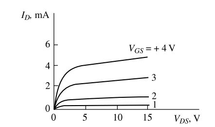
To analyze this, we plot versus for various levels of :
-
Case 1:
Here, is the threshold voltage, and the effective voltage () is given by:
- When is increased beyond a certain level, the drain current becomes constant, which is known as the pinch-off condition.
-
Case 2:
When is greater than , the conductivity of the MOSFET is higher with , implying:
The slope of the versus curve for is steeper than for .
Regions on the Graph:
- Saturation Region: The region where the drain current () is constant despite increases in .
- Triode Region: The region where increases with before reaching saturation.
- Cut-off Region: When is below the threshold voltage (), the MOSFET is OFF, and is zero.
2. Transfer Characteristics of Enhancement Type MOSFET:
Transfer characteristics describe the relationship between the output current () and the gate-source voltage () for a fixed . The transfer characteristic curve shows how the drain current changes as the gate voltage varies.
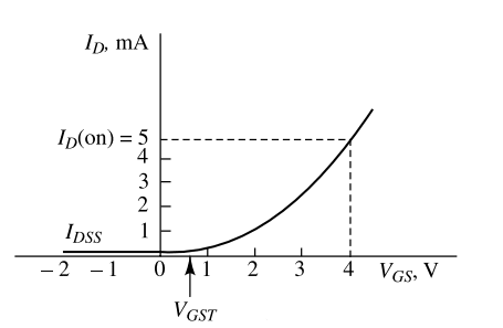
In this graph, when is below the threshold voltage , the MOSFET remains OFF, and is minimal.
Depletion Type MOSFET
1. Drain Characteristics:
Drain characteristics describe the relationship between and for different gate-source voltages ().
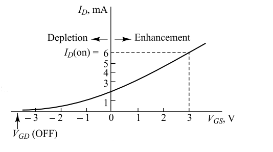
2. Transfer Characteristics:
Transfer characteristics describe the relationship between and for a fixed . This curve illustrates how the drain current changes with gate voltage, showing the MOSFET's behavior in different operating regions. Whenever the value is positive, the no. of electrons within the channel will increase. When the is positive then this region is the enhancement region. Similarly, when the is negative then this region is known as the depletion region.
Switching Characteristics of MOSFETs
| MOSFET | |||
|---|---|---|---|
| P-channel enhancement type | ON | OFF | OFF |
| N-channel enhancement type | OFF | OFF | ON |
| P-channel depletion type | ON | ON | OFF |
| N-channel depletion type | OFF | ON | ON |
Explanation:
-
P-channel Enhancement Type:
- : The MOSFET is ON because applying a negative gate-source voltage enhances the channel formation.
- : The MOSFET is OFF because there is no gate voltage to enhance the channel.
- : The MOSFET remains OFF because positive gate voltage does not enhance the channel in a P-channel enhancement MOSFET.
-
N-channel Enhancement Type:
- : The MOSFET is OFF because negative gate-source voltage prevents channel formation.
- : The MOSFET is OFF because no gate voltage means no channel enhancement.
- : The MOSFET is ON because positive gate voltage enhances the channel, allowing current flow.
-
P-channel Depletion Type:
- : The MOSFET is ON because a negative gate voltage does not deplete the channel.
- : The MOSFET is ON as the channel is already present.
- : The MOSFET is OFF because positive gate voltage depletes the channel, preventing current flow.
-
N-channel Depletion Type:
- : The MOSFET is OFF because negative gate voltage depletes the channel.
- : The MOSFET is ON because the channel is naturally present.
- : The MOSFET is ON as positive gate voltage can enhance the channel.
Advantages of MOSFET
- High Switching Speed : It can change its state rapidly from ON and OFF position.
- Low Power Consumption : Useful for battery operated devices.
- High input impedance : They use minimum input current.
- Low noise : They produce low noise and do not cause much disturbance.
Disadvantages of MOSFET
- Breakdown: MOSFETS have a very thin layer of gate oxide so on applying high voltage it can cause to breakdown of entire device.
- Temperature: Some functions of MOSFET are altered because of varying temperatures.
- Voltage capacity: They have a limited voltage capacity. -Expensive: Complex manufacturing of MOSFETS can lead to high cost of overall electronic device.
Applications of MOSFET
- Amplifiers: MOSFETs are used as an amplifiers in order to amplify weak signals.
- Switching power supplies: They are used as switches because they can alter power supply efficiently.
- Digital logic gates: They are used to build logic gates such as NAND, NOR etc.
- Voltage regulators: They are used as voltage regulators because they can control the amount of voltage.
- Memory devices: They are used in memory cells.