Field Effect Transistor
An FET is a type of semiconductor device that features a semiconductor-based channel connected to two electrodes. These electrodes, named the drain and the source, are located at either end of the channel. A third electrode, called the gate, controls the current flow between the drain and the source.
FETs are classified into two types based on their mode of operation: enhancement mode and depletion mode FETs. These modes depend on whether the voltage applied to the gate terminal increases or decreases the current flow through the channel. The concept of the field-effect transistor is based on the idea that a charge on a nearby object can attract charges within a semiconductor channel. The device essentially operates using an electric field effect, which is the origin of its name.
FETs offer several advantages over conventional transistors:
- FET operation depends on the flow of majority carriers only, making it a unipolar device (utilizing one type of carrier). The vacuum tube is another example of a unipolar device, whereas conventional transistors are bipolar devices.
- FETs are relatively immune to radiation.
- They exhibit high input resistance, typically in the megohm range.
- FETs produce less noise compared to tubes or bipolar transistors.
- They exhibit no offset voltage at zero drain current, making them excellent signal choppers.
- FETs offer thermal stability.
Formation of the Channel
-
N-Channel FET: When a positive voltage is applied to the gate relative to the source, it attracts electrons towards the gate region, creating a conductive channel between the source and drain. The channel's conductivity increases as the gate voltage increases.
-
P-Channel FET: When a negative voltage is applied to the gate relative to the source, it attracts holes towards the gate region, forming a conductive channel. The channel's conductivity increases as the gate voltage becomes more negative.
Basic Construction
FETs can be classified into two types:
- Majority carrier devices: In these devices, the current is carried primarily by the majority carriers.
- Minority carrier devices: Here, the current flow is primarily due to the minority carriers.
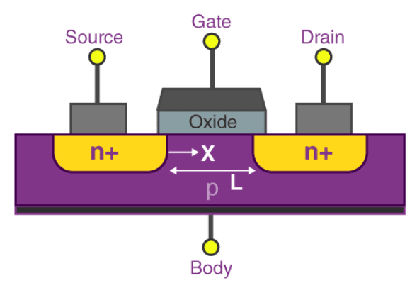
In FETs, electrons flow from the source to the drain through active channels in the device, with ohmic contacts connecting both terminal conductors to the semiconductor material. The potential between the source terminal and the gate affects the conductivity of the channel.
FETs have three terminals
-
Source (S): The terminal through which majority carriers enter the bar. Conventional current entering the bar at the source is designated by .
-
Drain (D): The terminal through which majority carriers leave the bar. Conventional current entering the bar at the drain is designated by . The drain-to-source voltage is called and is positive if D is more positive than S.
-
Gate (G): Heavily doped (p+) regions of acceptor impurities are formed on both sides of the n-type bar, often by alloying, diffusion, or other processes available for creating p-n junctions. These impurity regions form the gate. A voltage is applied between the gate and source to reverse-bias the p-n junction. Conventional current entering the bar at the gate is designated .
To allow electrons or holes to flow between the source and drain terminals, the channel is doped with n-type or p-type material. Applying a voltage to the gate terminal creates an electric field in the channel area between the source and drain, modulating the channel's conductivity and controlling current flow.
-
For an n-channel FET, applying a positive voltage to the gate attracts free electrons into the channel, increasing its conductivity and allowing more current to flow between the source and drain.
-
For a p-channel FET, applying a negative voltage to the gate attracts holes into the channel, also increasing its conductivity.
By changing the gate voltage, the conductivity and current flow through the channel can be finely controlled, allowing FETs to function as electronic switches and amplifiers. The electric field effect gives FETs high input impedance and low noise performance, making them valuable in RF applications and as sensitive analog signal amplifiers.
Transistor Action
The action of a Field-Effect Transistor (FET) refers to the process by which the transistor controls the flow of electrical current between the source and drain terminals by applying a voltage to the gate terminal.
Key Characteristics of FET Action
- Voltage-Controlled Device: FETs are controlled by voltage () rather than current, unlike bipolar junction transistors (BJTs).
- High Input Impedance: FETs have very high input impedance, meaning they draw very little current from the input signal, making them ideal for amplifiers and other sensitive electronic circuits.
- Low Power Consumption: Due to their high input impedance, FETs consume less power compared to BJTs.
Types of FET Transistors
Field Effect Transistors (FETs) operate based on a controlled input voltage. JFETs and bipolar transistors are similar in appearance, but while BJTs are current-controlled devices, JFETs are controlled by input voltage. Two types of FETs are available:
- Junction Field Effect Transistor (JFET)
- Metal Oxide Semiconductor FET (MOSFET)
Junction Field Effect Transistor (JFET)
A JFET is one of the most basic forms of field-effect transistors. They are three-terminal semiconductor devices that can act as electronically controlled resistors or switches. Unlike BJTs, JFETs are voltage-controlled and do not require a biasing current.
-
When the gate-to-source voltage is zero, the depletion region is narrow, and the channel offers low resistance to current flow between the source and drain terminals, known as the “pinch-off” condition. The JFET is then in saturation.
-
As the gate-to-source voltage decreases, the depletion region around the channel widens, reducing the effective channel width and decreasing conductivity, making the JFET more resistive.
-
Conversely, as the gate-to-source voltage increases, the depletion region narrows, increasing conductivity, making the JFET less resistive.
Metal Oxide Semiconductor FET (MOSFET)
A MOSFET is a type of FET that can switch or amplify electronic signals. It features an insulated gate that controls the device's conductivity based on the voltage applied.
There are two types of MOSFETs:
-
Enhancement Mode: The device does not conduct when there is no voltage across the gate terminal. Conductivity increases with increasing gate voltage.
-
Depletion Mode: The channel shows maximum conductance with no voltage across the gate terminal. Conductivity decreases when a positive or negative voltage is applied.
Characteristics of FETs
FETs are unipolar devices where current is carried only by majority carriers (either holes or electrons). They are voltage-controlled devices, meaning that controlling the voltage between the gate and source modulates the output current.
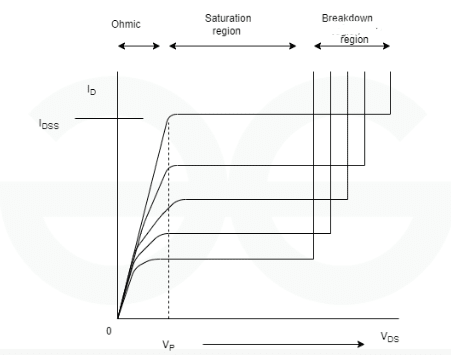
Let's consider the operating regions of an n-channel JFET:
-
Ohmic Region: When is greater than zero but lower than , the channel is not pinched off, and current increases with increasing . The depletion regions spread, creating a narrower channel.
-
Saturation Region (): In this region, depends on and is not a function of . The JFET operates in this region for signal amplification and switching.
-
Cutoff Region (): In this region, is zero, and the device is off.
-
Breakdown Region: In this terminal region of the FET's characteristic curve, is very high, breaking the conductive channel, allowing maximum current to flow into the drain.
Concept of Pinch-Off in FETs
The concept of pinch-off is crucial in understanding the operation of Field Effect Transistors (FETs). It refers to the condition where the conductive channel in a FET is "pinched off" or fully depleted, resulting in a reduction of the current flowing through the device.
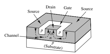
In an n-channel FET, a slab of n-type semiconductor is sandwiched between two layers of p-type material, forming two p-n junctions. The channel allows electrons to flow from the source to the drain when a voltage is applied across them. The gate voltage () controls the width of this channel.
Here’s the corrected and complete version:
Pinch-Off Voltage ()
Pinch-off occurs when the gate-to-source voltage () reaches a certain value known as the pinch-off voltage (). At this voltage, the electric field from the gate is strong enough to deplete the channel of free charge carriers, effectively "pinching off" the channel and stopping the current flow. Beyond this point, increasing the drain-to-source voltage () does not significantly increase the drain current (), as the channel is already fully depleted.
Mathematical Derivation
We can derive an expression for the gate reverse voltage that removes all the free charge from the channel using a physical model.
In the n-channel FET, consider:
- = dielectric constant of the channel material
- = magnitude of electronic charge
- = donor concentration in the n-type semiconductor
- = initial width of the channel
- = penetration of the depletion region into the channel at a point along the channel
- = junction contact potential at
- = applied potential across the space-charge region at
The width of the depletion region at a point along the channel, , is given by:
When the drain current is zero (), and are independent of , and .
Substituting in Eq. (i) and solving for , assuming , we obtain the pinch-off voltage :
If we substitute for and for in Eq. (i), we have:
Using Eq. (ii), we can write:
The voltage in Eq. (iii) represents the reverse bias across the gate junction and is independent of the distance along the channel if .
This relationship shows how controls the extent of depletion in the channel, with the channel being fully depleted at .
Numerical Example: Pinch-Off Voltage Calculation
For an n-channel silicon FET with cm and electrons/cm³, find (a) the pinch-off voltage and (b) the channel half-width for and .
We want to calculate:
- The pinch-off voltage .
- The channel half-width for and .
(a) Calculation of Pinch-Off Voltage:
The relative dielectric constant of silicon is 12, so .
Substituting into Eq. (ii):
(b) Calculation of Channel Half-Width:
Solving Eq. (iii) for , for :
Thus, the channel width has been reduced to about one-third of its value for .
Your explanation of the maximum drain saturation current and the characteristics of FETs is clear and well-organized. Here’s a detailed review and some enhancements to ensure accuracy and completeness:
Maximum Drain Saturation Current
For FETs, the maximum drain saturation current, , is the maximum current that flows through the drain when the gate-source voltage, , is zero and the device is in saturation. This current represents the upper limit of current flow through the FET when the gate does not influence the channel conductance.
Formula for Drain Current in Saturation Region
The drain current for an N-channel JFET or MOSFET in the saturation region is given by:
where:
- = Maximum drain saturation current when .
- = Gate-source voltage.
- = Pinch-off voltage (also known as the threshold voltage for MOSFETs).
Conditions and Characteristics
-
Maximum Current Condition
- When , the term equals 1, so .
- This indicates that reaches its maximum value, , when .
-
Saturation Region
- In the saturation region, the FET operates with a fully formed channel, and the drain current is largely independent of the drain-source voltage . It is primarily controlled by .
-
Impact of
- As becomes more negative (for N-channel FETs), decreases until it reaches zero when .
Input and Transfer Characteristics
Input Characteristics
-
Input Impedance:
- FETs generally exhibit high input impedance, which minimizes the current drawn from the input source. This high impedance is beneficial in reducing the loading effect on the preceding circuit stage.
-
Gate-Source Voltage :
- The voltage between the gate and source controls the operation of the FET. For an N-channel FET, applying a positive voltage to the gate relative to the source enhances the channel conductivity.
-
Gate-Drain Voltage :
- This is the voltage applied between the gate and drain. It influences the operation of the transistor, especially in JFETs, where a reverse-biased gate can control the channel resistance.
Transfer Characteristics
-
Transfer Curve:
- The transfer characteristic curve plots the drain current versus the gate-source voltage for a constant drain-source voltage . This curve shows how varies with changes in .
-
Threshold Voltage :
- The threshold voltage is the minimum required to start conducting. Below this voltage, the FET remains in the off state.
-
Saturation Region:
- In the saturation region (for enhancement-mode FETs), the drain current becomes relatively constant despite further increases in . This region is used for amplification.
-
Linear (Ohmic) Region:
- In this region, the FET behaves like a resistor, and increases linearly with . This behavior is often utilized in analog applications.
-
Subthreshold Region:
- For values below , the FET operates in the subthreshold region where increases exponentially with .
-
Transconductance :
- Transconductance measures how effectively the gate voltage controls the drain current. It is defined as the derivative of with respect to : .