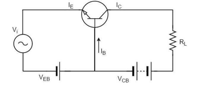
Transistor Biasing and Bias Stabilization
Operating Point
The proper flow of zero signal collector current and the maintenance of proper collector-emitter voltage during the passage of a signal is known as Transistor Biasing. The circuit that provides transistor biasing is called a Biasing Circuit.
Need for DC biasing
If a signal of very small voltage is applied to the input of a BJT, it cannot be amplified. This is because, for a BJT to amplify a signal, two conditions must be met:
- The input voltage should exceed the cut-in voltage for the transistor to be ON.
- The BJT should be in the active region to operate as an amplifier.
If appropriate DC voltages and currents are supplied to the BJT by external sources, ensuring the BJT operates in the active region while superimposing the AC signals to be amplified, this problem can be avoided. The given DC voltage and currents are chosen so that the transistor remains in the active region throughout the entire input AC cycle. Hence, DC biasing is necessary.
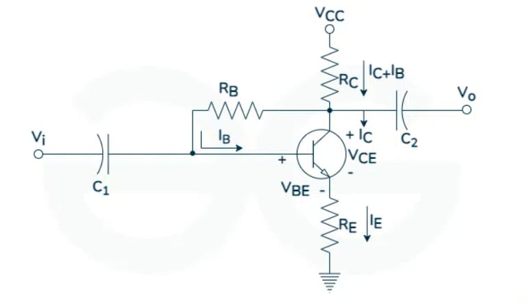
The below figure shows a transistor amplifier that is provided with DC biasing in both input and output circuits.
Operating Point
When a line is drawn connecting the saturation and cutoff points, it is called a Load Line. This line, when drawn over the output characteristic curve, intersects at a point known as the Operating Point.
This operating point is also called the quiescent point or simply the Q-point. There can be many such intersecting points, but the Q-point is selected in such a way that, irrespective of the AC signal swing, the transistor remains in the active region.
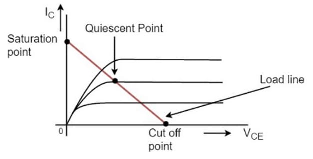
The operating point should not get disturbed, as it must remain stable to achieve faithful amplification. Hence, the quiescent point or Q-point is the value where Faithful Amplification is achieved.
Factors affecting the operating point
The main factor that affects the operating point is temperature. The operating point shifts due to changes in temperature.
As temperature increases, the values of , , and are affected.
So, the main problem affecting the operating point is temperature. Hence, the operating point should be made independent of temperature to achieve stability. To achieve this, biasing circuits are introduced.
Stability Factor
The process of making the operating point independent of temperature changes or variations in transistor parameters is known as Stabilization.
Once stabilization is achieved, the values of and become independent of temperature variations or transistor replacement. A good biasing circuit helps in the stabilization of the operating point.
Need for Stabilization
Stabilization of the operating point is necessary due to the following reasons:
- Temperature dependence of
- Individual variations
- Thermal runaway
-
Temperature Dependence of
The expression for collector current is:
The collector leakage current is greatly influenced by temperature variations. To counter this, the biasing conditions are set so that the zero signal collector current . Therefore, the operating point needs to be stabilized, i.e., it is necessary to keep constant.
-
Individual Variations
As the value of and the value of are not the same for every transistor, whenever a transistor is replaced, the operating point tends to change. Hence, it is necessary to stabilize the operating point.
-
Thermal Runaway
The expression for collector current is:
The flow of collector current, along with the collector leakage current, causes heat dissipation. If the operating point is not stabilized, a cumulative effect occurs, increasing this heat dissipation.
The self-destruction of such an unstabilized transistor is known as Thermal Runaway.
To avoid thermal runaway and the destruction of the transistor, it is necessary to stabilize the operating point, i.e., to keep constant.
Stability Factor
It is understood that should be kept constant despite variations in or . The extent to which a biasing circuit is successful in maintaining this is measured by the Stability Factor, denoted by .
By definition, the rate of change of collector current with respect to the collector leakage current at constant and is called the Stability Factor.
at constant and
Hence, we can understand that any change in collector leakage current greatly affects the collector current. The stability factor should be as low as possible so that the collector current doesn’t get affected. is the ideal value.
The general expression of the stability factor for a CE configuration can be obtained as follows:
Differentiating the above expression with respect to , we get:
Or:
Since:
Or:
Hence the stability factor depends on , and .
Methods of Transistor Biasing
Biasing in transistor circuits is typically done using two DC sources: and . However, it is more economical to minimize the number of DC sources to one, which also simplifies the circuit.
The commonly used methods of transistor biasing are:
- Fixed bias circuit (Single Base Resistor Biasing) or base bias
- Collector-to-base bias
- Biasing with collector feedback resistor
- Voltage-divider bias circuit (V.D.B) or self-bias
- Emitter bias or modified fixed bias circuit
All of these methods share the basic principle of obtaining the required value of and from under zero signal conditions.
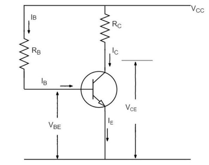
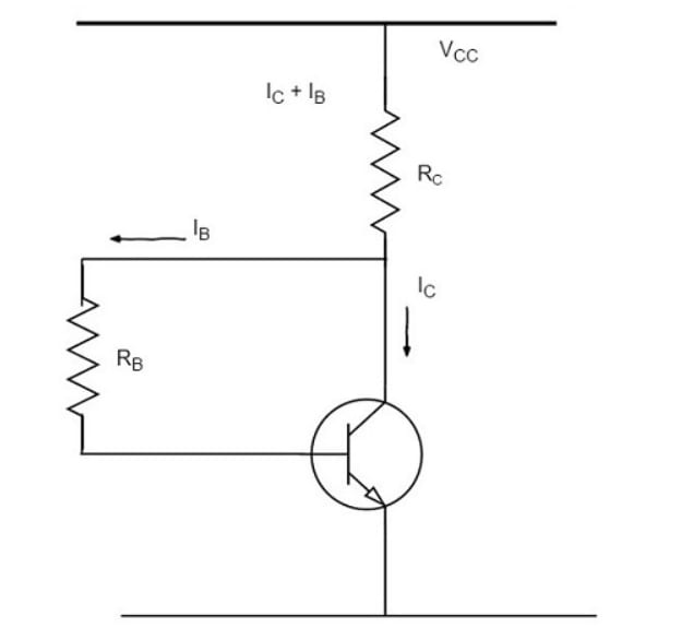
Fixed Bias Circuit (Single Base Resistor Biasing) or Base Bias
In this method, as the name implies, a resistor with high resistance is connected to the base. The required zero signal base current is provided by , which flows through . The base-emitter junction is forward biased since the base is positive with respect to the emitter.
The required value of zero signal base current and, consequently, the collector current (since ) can be achieved by selecting the appropriate value of the base resistor . Therefore, it is necessary to determine the value of . The figure below shows the base resistor method of biasing.
Let be the required zero signal collector current. Therefore:
Considering the closed circuit from through the base, emitter, and ground, and applying Kirchhoff’s voltage law, we get:
Or:
Therefore:
Since is generally quite small compared to , it can be neglected with minimal error. Then:
We know that is a fixed, known quantity, and is chosen at a suitable value. Since can be found directly, this method is called the fixed bias method.
Stability Factor
The stability factor is given by:
In the fixed-bias method of biasing, is independent of , so:
Substituting this value into the equation, the stability factor becomes:
Thus, the stability factor in a fixed bias circuit is , which means that changes times as much as any change in .
Advantages:
- The circuit is simple.
- Only one resistor is required.
- Biasing conditions are easily set.
- There is no loading effect, as no resistor is present at the base-emitter junction.
Disadvantages:
- Stabilization is poor, as heat development cannot be controlled.
- The stability factor is very high, increasing the risk of thermal runaway.
Collector-to-Base Bias
The collector-to-base bias circuit is similar to the base bias circuit, except that the base resistor is connected to the collector rather than the supply.
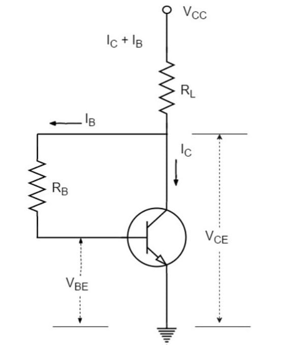
This circuit helps improve stability significantly. If the value of increases, the voltage across increases, which in turn reduces the base current . This action compensates for the original increase in .
The required value of needed to provide the zero signal collector current can be calculated as follows:
The voltage drop across will be:
From the figure:
Or:
Therefore:
Or:
Applying Kirchhoff's Voltage Law (KVL):
Or:
Therefore:
Since is almost independent of collector current, we get:
We know that:
Therefore:
This value is smaller than , which is obtained for the fixed bias circuit, indicating an improvement in stability.
This circuit provides negative feedback, which reduces the gain of the amplifier. Thus, the increased stability of the collector-to-base bias circuit is obtained at the cost of AC voltage gain.
Advantages of the Collector-to-Base Bias Circuit:
- Simple circuit design.
- Provides some stabilization of the operating point.
- Requires only one resistor at the base.
- Reduced sensitivity to transistor variations.
- Lower sensitivity to power supply changes.
Disadvantages of the Collector-to-Base Bias Circuit:
- Does not provide optimal stabilization, as the stability factor is high.
- Negative feedback reduces the gain of the amplifier.
- Dependency on component matching.
- More complex compared to fixed bias circuits.
- Limited use in certain applications with specific voltage requirements.
Biasing with Collector Feedback Resistor
In this method, the base resistor has one end connected to the base and the other to the collector, as the name implies. In this circuit, the zero signal base current is determined by rather than by .
forward-biases the base-emitter junction, causing base current to flow through , which in turn causes the zero signal collector current to flow in the circuit. The figure below shows the biasing with a collector feedback resistor circuit.
The required value of needed to provide the zero signal collector current can be determined as follows:
Or:
Since:
Alternatively:
Or:
Since:
Where:
Mathematically, the stability factor is:
Therefore, this method provides better thermal stability than the fixed bias method.
The Q-point values for the circuit are:
Advantages:
- The circuit is simple, requiring only one resistor.
- Provides some stabilization for lesser changes.
Disadvantages:
- The circuit does not provide strong stabilization.
- The circuit provides negative feedback, which reduces the gain.
Voltage-Divider Bias Circuit (V.D.B) or Self-Bias
Among all methods of providing biasing and stabilization, the voltage-divider bias method is the most commonly used. In this method, two resistors and are connected to to provide biasing, while the resistor in the emitter provides stabilization.
The name "voltage divider" comes from the voltage divider formed by and . The voltage drop across forward-biases the base-emitter junction, which causes the base current and hence the collector current to flow under zero signal conditions. The figure below shows the circuit of the voltage-divider bias method.

Suppose the current flowing through resistance is . Since the base current is very small, it can be assumed with reasonable accuracy that the current flowing through is also .
Collector Current, :
From the circuit, it is evident that:
Therefore, the voltage across resistance is:
Applying Kirchhoff’s Voltage Law (KVL) to the base circuit:
Since :
From the above expression, it is evident that doesn’t depend on . is very small, so doesn’t get affected by at all. Thus, in this circuit is almost independent of transistor parameters, and good stabilization is achieved.
Collector-Emitter Voltage,
Applying KVL to the collector side:
Since :
Therefore:
provides excellent stabilization in this circuit.
Suppose there is a rise in temperature; the collector current increases, which causes the voltage drop across to increase. As the voltage drop across is , which is independent of , the value of decreases. The reduced value of tends to restore to its original value.
Stability Factor
The equation for the Stability Factor of this circuit is obtained as:
Stability Factor:
Where:
If the ratio is very small, then can be neglected compared to 1, and the stability factor becomes:
Stability Factor:
This is the smallest possible value of and leads to the maximum possible thermal stability.
Emitter Bias or Modified Fixed Bias Circuit
In this configuration, a resistor is added from the emitter to the ground terminal of the fixed bias circuit. This is done to improve the stability of the circuit.
Base Circuit:
Applying KVL to this circuit:
But:
and:
Substituting the value of into , we get:
Now, substituting the value of into :
Collector Circuit:
Applying KVL to this circuit:
Since :
Where:
Advantages of the Modified Fixed Bias Circuit:
- The addition of the emitter resistor provides improved stability.
- It offers a high voltage gain.
- It is a simple circuit with enhanced stabilization.
- Reduced sensitivity to transistor variations.
- It strikes a balance between simplicity and performance.
Disadvantages of the Modified Fixed Bias Circuit:
- The operating point can be affected by changes in temperature.
- It requires the use of a dual polarity power supply.
- Limited voltage range.
- Potential issues with component matching.
- More complex than a simple fixed bias circuit.
Bipolar Junction Transistors
Transistor operation and current components in p- n- p and n- p- n transistors , input/output characteristics of CB and CE configurations,Transistor as an Amplifier ,transistor cutoff , saturation and active regions
Field Effect Transistors
Basic construction, transistor action, concept of pinch off, maximum drain saturation current, input and transfer characteristics, current, input and transfer characteristics