What is a Transistor?
A transistor is a semiconductor device that can amplify or switch electronic signals and power. Transistors are made of materials like silicon or germanium that allow electrical current to flow through them in a controlled manner.
Types of Transistors
Transistors are primarily categorized into two types:
- Bipolar Junction Transistors (BJT): BJT is a three-terminal semiconductor device used for signal amplification and switching. Based on the arrangement of semiconductor layers and the direction of current flow, BJTs are classified as NPN (Negative-Positive-Negative) or PNP (Positive-Negative-Positive). In NPN transistors, the majority carriers are electrons, while in PNP transistors, the majority carriers are holes.
- Field Effect Transistors (FET): FET is a semiconductor device controlling the flow of electrical current in electronic circuits. FETs modulate the electrical field within a semiconductor, enabling them to function as voltage-controlled switches or amplifiers.
Examples of NPN and PNP transistors include their use in amplifier circuits, switching applications, voltage regulation, and oscillators.
Bipolar Junction Transistors (BJTs)
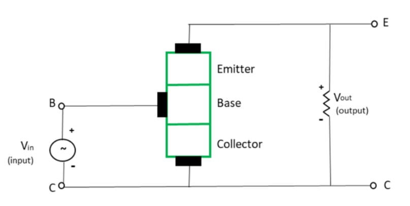
A bipolar junction transistor (BJT) is a semiconductor device used in electronic circuits for amplifying or switching signals. It comprises three doped semiconductor regions: the emitter, the base, and the collector. The flow of current between the emitter and the collector is regulated by the current or voltage applied to the base region.
Structure:
- Emitter (E): This region injects majority carriers (either electrons or holes) into the transistor.
- Base (B): A thin region sandwiched between the emitter and collector, controlling the current flow through the transistor. The base current, controlled by the voltage applied to the base terminal, regulates the flow of majority carriers from the emitter to the collector.
- Collector (C): Collects majority carriers emitted by the emitter and controls the output current of the transistor.
Types of BJTs:
- NPN Transistor: The emitter is N-type semiconductor, the base is P-type semiconductor, and the collector is N-type.
- PNP Transistor: The emitter is P-type semiconductor, the base is N-type, and the collector is P-type semiconductor.
Transistor Operation and Current Components in p-n-p and n-p-n Transistors
PNP Transistor
A PNP transistor is a bipolar junction transistor constructed by sandwiching an N-type semiconductor between two P-type semiconductors. A PNP transistor has three terminals - a Collector (C), Emitter (E) and Base (B). The PNP transistor behaves like two PN junction diodes connected back to back.
Symbol of PNP Transistor
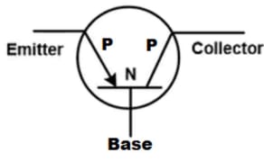
In P-type semiconductors, the majority charge carriers are holes. Therefore, in the PNP transistor, the formation of the current is due to the movement of holes. The middle layer (N-type layer) is called the Base terminal (B). The left P-type layer works as an Emitter terminal (E) and the right P-type layer works as a Collector terminal (C).
Construction of PNP Transistor
The Emitter and Collector layers in a PNP transistor are heavily doped with acceptor impurities, resulting in a higher concentration of charge carriers (holes) compared to the Base layer. This heavy doping creates a wider depletion region at both the Emitter-Base and Collector-Base junctions, extending further into the lightly doped Base layer. While the Emitter and Collector regions typically have larger areas compared to the Base region, it's important to note that this may vary depending on the specific transistor design.
In N-type semiconductors, such as the Base layer in a PNP transistor, there are a significant number of free electrons. However, due to the Base layer being lightly doped, the concentration of free electrons is significantly lower compared to the heavily doped Emitter and Collector regions. This difference in doping levels and charge carrier concentrations enables the Base region to act as a barrier, regulating the flow of majority charge carriers (holes) from the Emitter to the Collector.
Working of PNP Transistor
A PNP transistor operates based on the biasing of its junctions and the movement of majority charge carriers (holes). Here's a breakdown of its working principle:
-
Biasing of Junctions:
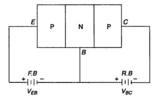
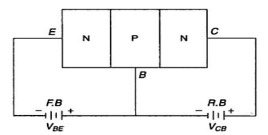
- The Emitter-Base junction is forward biased by connecting the positive terminal of a voltage source () to the Emitter (P-type) and the negative terminal to the Base (N-type). Conversely, the Collector-Base junction is reverse biased by connecting the positive terminal of a voltage source () to the Base and the negative terminal to the Collector (P-type).
-
Depletion Region:
- Due to the forward biasing of the Emitter-Base junction, the depletion region at this junction is narrow, allowing for the easy flow of majority charge carriers (holes) from the Emitter to the Base. In contrast, the reverse biasing of the Collector-Base junction widens the depletion region at this junction, hindering the flow of majority charge carriers from the Base to the Collector.
-
Current Flow:
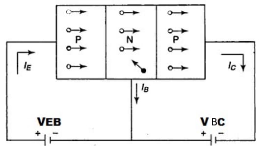
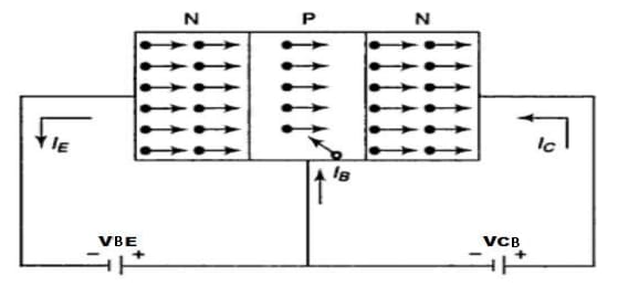
- Holes from the Emitter region cross the narrow depletion region and enter the Base layer. Some of these holes recombine with electrons in the Base, while the remaining holes continue to the Collector region, constituting the Collector current ().
- The current flowing through the Emitter-Base junction, known as the Emitter current (), is primarily due to the movement of holes, which are the majority charge carriers in the transistor.
- Additionally, a portion of the holes that enter the Base region contributes to the Base current (). This current, while typically smaller than the Emitter and Collector currents, plays a crucial role in modulating the transistor's operation and controlling its amplification and switching characteristics.
-
Base Voltage and Transistor Operation:
- To enable conduction in the transistor, the Base voltage must be sufficiently negative relative to the Emitter voltage. However, the specific threshold voltage required for proper operation depends on the transistor's characteristics and desired mode of operation.
- If the Base voltage is significantly lower than the Emitter voltage, the transistor will be in the cut-off region, resulting in no current flow. Conversely, if the Base voltage is above the threshold for forward biasing the Emitter-Base junction, current may flow through the transistor, although at a reduced level.
In summary, a PNP transistor conducts current primarily through the movement of majority charge carriers (holes) from the Emitter to the Collector, controlled by the biasing of its junctions. Proper biasing and voltage levels are essential for regulating the transistor's operation and enabling desired circuit behavior.
In a PNP transistor, the currents consist of three main components:
-
Emitter Current (): This is the total current entering the transistor at the emitter terminal. The majority of IE is due to the flow of holes (majority carriers in PNP) from the emitter to the base. A small portion of IE also consists of minority carrier electrons moving from the base to the emitter.
-
Collector Current (): This is the main output current leaving the transistor at the collector terminal. It primarily consists of holes that originate from the emitter and diffuse across the collector-base junction, reaching the collector.
A small portion of these holes may recombine with electrons in the base region. -
Base Current (): This is the current flowing into the base terminal. It's composed of holes from the emitter that enter the base region. Some of these holes recombine with electrons in the base, while the remaining holes contribute to the collector current. The base current plays a crucial role in controlling the flow of a much larger collector current.
NPN Transistor
An NPN transistor is a type of bipolar junction transistor commonly used in electronic circuits. It is constructed by sandwiching a thin P-type semiconductor layer between two thicker N-type semiconductor layers. The transistor has three terminals: Collector (C), Emitter (E), and Base (B). It functions similarly to two PN junction diodes connected back to back.
Symbol of NPN Transistor
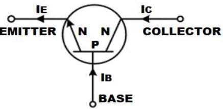
The arrowhead in the transistor symbol indicates the conventional direction of current flow: Collector current (), Base current (), and Emitter current ().
Construction of NPN Transistor
In an NPN transistor, the Emitter and Collector regions are heavily doped compared to the lightly doped Base region. This heavy doping of the Emitter allows it to inject a large number of charge carriers (electrons) into the Base. The Base, being thin and lightly doped, serves to control the flow of these charge carriers from the Emitter to the Collector.
Working of NPN Transistor
The operation of an NPN transistor involves the biasing of its junctions and the flow of charge carriers through the semiconductor regions:
-
Biasing of Junctions:
- The Base-Emitter junction is forward biased by applying a positive voltage () to the Emitter terminal and a negative voltage to the Base terminal.
- Conversely, the Collector-Base junction is reverse biased by applying a positive voltage () to the Collector terminal and a negative voltage to the Base terminal.
-
Depletion Regions:
- The forward biasing of the Base-Emitter junction results in a thin depletion region, allowing electrons to flow from the heavily doped N-type Emitter to the lightly doped P-type Base.
- In contrast, the reverse biasing of the Collector-Base junction widens the depletion region, preventing the flow of majority carriers (electrons) from the Base to the Collector.
-
Current Flow:
- Electrons injected from the Emitter into the Base region constitute the Emitter current (). Most of these electrons traverse the Base and enter the Collector region.
- A small portion of electrons recombine with holes in the Base, contributing to the Base current (). The Base current is relatively small compared to the Emitter current.
- The electrons that pass through the Base reach the Collector region, constituting the Collector current (). The Collector current is typically much larger than the Base current.
In summary, an NPN transistor operates by controlling the flow of electrons from the Emitter to the Collector through the Base region. Proper biasing of the junctions and modulation of currents enable the transistor to amplify signals and perform various electronic functions.
In an NPN transistor, the currents consist of three main components:
-
Emitter Current (): This is the total current entering the transistor at the emitter terminal. The majority of is due to the flow of electrons injected from the heavily doped N-type emitter into the lightly doped P-type base. Some electrons recombine with holes in the base, contributing to the base current (), while the majority continue into the collector region.
-
Base Current (): This is the current flowing into the base terminal. It's primarily composed of electrons that diffuse from the emitter into the base region due to the forward bias. Some of these electrons recombine with holes in the base, contributing to the base current, while the remaining electrons continue into the collector region. The base current plays a crucial role in controlling the flow of a much larger collector current.
-
Collector Current (): This is the main output current leaving the transistor at the collector terminal. It consists of electrons that traverse the base region and enter the collector region. The collector current is primarily composed of electrons that have passed through the base without recombining with holes. While a very small portion of the collector current may result from some recombination effects in the base, this is negligible compared to the dominant flow of electrons from the emitter.
Input/Output Characteristics of CB and CE Configurations
Configurations of BJT
A transistor has three terminals. Any of these three terminals could be connected to form the common input and output terminal. Depending upon the terminal, which is used as common terminal, there are three types of transistor configurations:
- Common-Base Configuration (CB Configuration)
- Common-Emitter Configuration (CE Configuration)
- Common-Collector Configuration (CC Configuration)
Common-Base Configuration (CB Configuration)
It is not a single video but a playlist, and it contains three videos. When one video finishes, the next will play automatically.
In this type of configuration, the base terminal of the transistor serves as a common terminal, so it is called as common-base (CB) configuration. The input voltage is applied between base and emitter terminal. The output is taken between collector and base terminal of the device. Common-base configuration has low input resistance but a high output resistance. Current gain in common-base configuration is denoted by Greek letter (alpha). It is defined as the ratio of collector current to the emitter current. Mathematically, it is represented as:
As the collector current is always smaller than emitter current, so the current gain in common-emitter configuration is always less than unity.
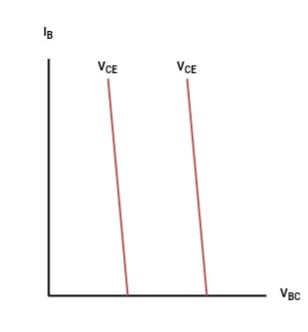
Input Characteristics of Common-Base Configuration
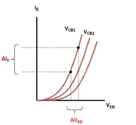
The input characteristics of a Common Base (CB) configuration describe the relationship between the emitter current and the emitter-base voltage for different values of the collector-base voltage .
-
Input Signal: The input signal is applied between the emitter and base terminals.
-
Input Impedance: The input impedance of the common-base configuration is typically low, which means that a small change in the input voltage causes a relatively large change in the input current .
-
Input Characteristic Curve:
Plotting the Curve: The input characteristic curve is plotted between the emitter current on the y-axis and the emitter-base voltage on the x-axis for various values of the collector-base voltage .
Diode-like Behavior: The input characteristic curve resembles that of a forward-biased diode, showing that as increases, also increases, especially after a certain threshold (typically around 0.7V for silicon transistors).
-
Effect of : The input characteristics are slightly influenced by changes in . However, the effect is generally minimal, meaning that for a wide range of , the input characteristics remain similar.
-
Non-Linear Relationship: The relationship between and is non-linear due to the exponential nature of the emitter-base junction, which is a PN junction.
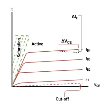
Output Characteristics of Common-Base Configuration
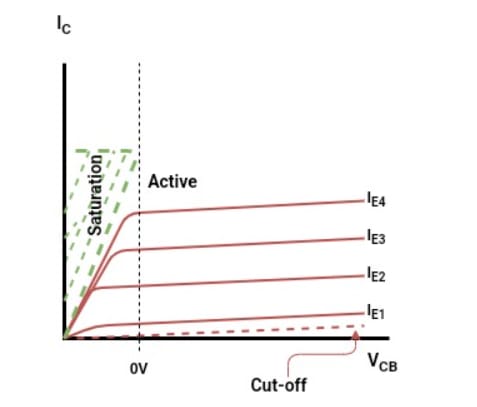
The output characteristics of a Common Base (CB) configuration describe the relationship between the collector current and the collector-base voltage for different values of emitter current .
-
Output Signal: The output signal is taken from the collector-base junction.
-
Output Impedance: The output impedance of the common-base configuration is typically high, which means that the circuit resists changes in output current with variations in output voltage .
-
Output Characteristic Curve:
Plotting the Curve: The output characteristic curve is plotted between the collector current on the y-axis and the collector-base voltage on the x-axis for various values of emitter current .
Regions of Operation: The output characteristic curve typically shows three distinct regions:
Cut-off Region: In this region, the collector current is very small (almost zero) because the emitter-base junction is not forward biased enough, and the transistor is in the off state.
Active Region: In this region, the transistor operates normally, and the collector current is largely independent of but depends on the emitter current . This is the region where the transistor is typically used for amplification.
Saturation Region: In this region, the collector current is high, and the transistor is fully on. The is very low, and the transistor cannot increase much more despite increases in .
-
Current Gain : The current gain in a common-base configuration is denoted by , which is the ratio of the collector current to the emitter current . is typically slightly less than 1, as most of the emitter current is transferred to the collector.
-
Linear Region: In the active region, the transistor exhibits a linear relationship between the collector current and the emitter current, making it suitable for amplification.
Common-Emitter Configuration (CE Configuration)
It is not a single video but a playlist, and it contains three videos. When one video finishes, the next will play automatically.
This type of configuration is called as common-emitter (CE) configuration as the emitter terminal of the transistor is made as a common terminal. The input voltage is applied between base and emitter terminal of the transistor. The output is obtained between emitter and collector terminal. Common-emitter configuration has a low input resistance but very high output resistance. Current gain in common-emitter configuration is denoted by a Greek letter (beta). It is defined as the ratio of collector current to the base current. Mathematically, it is represented as:
As the value of collector current is much larger than that of base current, so the current gain in common-emitter configuration is very large (greater than unity). The value of ranges between 20 to 300.
Input Characteristics of Common-Emitter Configuration
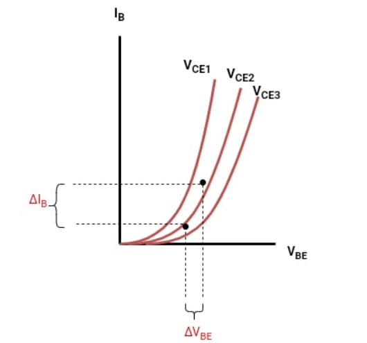
-
Input Impedance: The input impedance in the common-emitter configuration is typically moderate. It depends on the base resistance and the dynamic resistance of the base-emitter junction. It is usually in the range of a few hundred to a few thousand ohms.
-
Base-Emitter Voltage : The input characteristic curve shows the relationship between the base-emitter voltage and the base current for different values of collector-emitter voltage . typically ranges between 0.6V to 0.7V for silicon transistors when the transistor is in the active region.
-
Base Current : The input current is the base current, . The base current is small because the transistor operates with a high current gain , where . is controlled by the base-emitter voltage and is generally in the microampere to milliampere range.
-
Effect of Collector-Emitter Voltage : The input characteristics are slightly affected by changes in . Higher slightly decreases for a given , a phenomenon known as the Early effect.
Output Characteristics of Common-Emitter Configuration
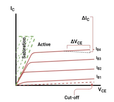
-
Output Impedance: The output impedance of a common-emitter amplifier is moderately high but generally lower than that of a common-base configuration. It is primarily determined by the collector resistance and the transistor's intrinsic properties.
-
Collector-Emitter Voltage : The output characteristic curve plots the relationship between the collector-emitter voltage and the collector current for different values of base current .
For a given base current, the collector current increases with the collector-emitter voltage until it reaches saturation. -
Collector Current : The output current is the collector current, . In the active region, is relatively constant and is controlled by the base current .
The collector current is a function of the base current and the transistor’s current gain , where . -
Effect of Base Current : The collector current increases with an increase in base current . The output characteristic curves shift upward as the base current increases.
-
Saturation Region: In the saturation region, as decreases to a low value, the collector current becomes limited by the external circuit, and the transistor may enter saturation, where is minimal.
-
Relation Between and : Mathematically, the relationship between and is represented as:
OR
where,
- = current gain in common-base configuration.
- = current gain in common-emitter configuration.
Common-Collector Configuration (CC Configuration)
This type of configuration is called as common-collector (CC) configuration as the collector terminal of the transistor is made as a common terminal. The input voltage is applied between base and collector terminal of the transistor. The output is obtained between emitter and collector terminal of the transistor. Common-collector terminal has a very high input resistance but a low output resistance. Current gain in common-collector configuration is denoted by Greek letter (gamma). It is defined as the ratio of emitter current to the base current. Mathematically, it is represented as:
Relationship between and and :
Mathematically, the relationship of with and is represented as:
where,
- = current gain in common-base configuration.
- = current gain in common-emitter configuration.
- = current gain in common-collector configuration.
Input Characteristics of Common-Collector Configuration
-
Input Impedance: The input impedance of a common-collector amplifier is typically high. It is mainly determined by the base-emitter junction and the transistor's intrinsic properties. It often ranges from a few kilo-ohms to several kilo-ohms, which makes it suitable for impedance matching applications.
-
Base-Collector Voltage : The input characteristic curve shows the relationship between the base-collector voltage () and the base current , with the collector-emitter voltage being relatively constant. typically ranges between 0.6V to 0.7V for silicon transistors when the transistor is in the active region.
-
Base Current : The input current is the base current, . In the common-collector configuration, is relatively small because the transistor operates with a high current gain , where . is controlled by the base-collector voltage and is generally in the microampere to milliampere range.
-
Effect of Collector-Emitter Voltage : The input characteristics are not significantly affected by changes in , as the common-collector configuration maintains a nearly constant voltage drop across the base-emitter junction. The voltage drop across the base-emitter junction is relatively stable, making the configuration useful for buffering applications.
Output Characteristics of Common-Collector Configuration
-
Output Impedance: The output impedance of a common-collector amplifier is typically low. This is due to the emitter follower configuration, where the emitter resistor plays a significant role in reducing impedance. It often ranges from a few ohms to a few hundred ohms, making it suitable for driving low-impedance loads.
-
Collector-Emitter Voltage : In the common-collector configuration, the collector-emitter voltage is relatively high and is not a critical parameter for determining the output characteristics. The is generally kept constant because the transistor is operating in the active region, and changes in have minimal impact on the output characteristics.
-
Emitter Current : The output current is the emitter current, , which is approximately equal to the collector current plus the base current . In the active region, closely follows the input current due to the high current gain of the transistor.
-
Voltage Gain: The common-collector configuration provides a voltage gain slightly less than 1 (unity gain). The output voltage is approximately equal to the input voltage minus the base-emitter voltage drop . The gain is typically close to 1, with the primary function being impedance matching rather than amplification.
-
Effect of Base Current : The output characteristics are influenced by the base current . Changes in affect the emitter current , which in turn affects the output voltage. The output voltage is affected by the base current due to the relationship between the emitter current and the base current.
Transistor as an Amplifier
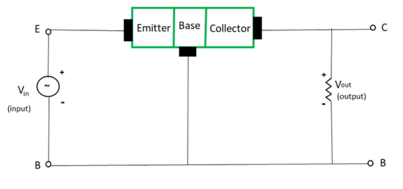
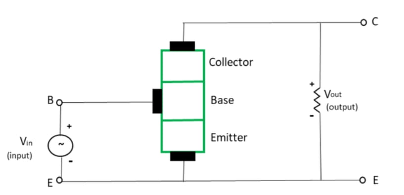
A transistor acts as an amplifier by raising the strength of a weak signal. The DC bias voltage applied to the emitter base junction, makes it remain in forward biased condition. This forward bias is maintained regardless of the polarity of the signal. The below figure shows how a transistor looks like when connected as an amplifier.
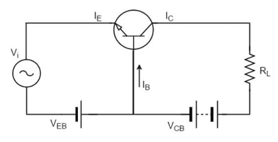
The low resistance in input circuit, lets any small change in input signal to result in an appreciable change in the output. The emitter current caused by the input signal contributes the collector current, which when flows through the load resistor RL, results in a large voltage drop across it. Thus a small input voltage results in a large output voltage, which shows that the transistor works as an amplifier.
Performance of Amplifier
As the common emitter mode of connection is mostly adopted, let us first understand a few important terms with reference to this mode of connection.
-
Input Resistance: As the input circuit is forward biased, the input resistance will be low. The input resistance is the opposition offered by the base-emitter junction to the signal flow. By definition, it is the ratio of small change in base-emitter voltage to the resulting change in base current at constant collector-emitter voltage. Input resistance,
Where = input resistance, = base-emitter voltage, and = base current.
-
Output Resistance: The output resistance of a transistor amplifier is very high. The collector current changes very slightly with the change in collector-emitter voltage. By definition, it is the ratio of change in collector-emitter voltage to the resulting change in collector current at constant base current.
Output resistance,
Where = Output resistance, = Collector-emitter voltage, and = Collector-emitter voltage.
-
Effective Collector Load: The load is connected at the collector of a transistor and for a single-stage amplifier, the output voltage is taken from the collector of the transistor and for a multi-stage amplifier, the same is collected from a cascaded stages of transistor circuit. By definition, it is the total load as seen by the a.c. collector current. In case of single stage amplifiers, the effective collector load is a parallel combination of RC and Ro.
Effective Collector Load,
Hence for a single stage amplifier, effective load is equal to collector load RC. In a multi-stage amplifier (i.e. having more than one amplification stage), the input resistance Ri of the next stage also comes into picture. Effective collector load becomes parallel combination of , and i.e,
Effective Collector Load,
As input resistance Ri is quite small, therefore effective load is reduced.
-
Current Gain: The gain in terms of current when the changes in input and output currents are observed, is called as Current gain. By definition, it is the ratio of change in collector current to the change in base current .
Current gain,
The value of ranges from 20 to 500. The current gain indicates that input current becomes times in the collector current.
-
Voltage Gain: The gain in terms of voltage when the changes in input and output currents are observed, is called as Voltage gain. By definition, it is the ratio of change in output voltage to the change in input voltage .
Voltage gain,
For a single stage, .
However, for Multistage,
Where is the input resistance of the next stage.
-
Power Gain: The gain in terms of power when the changes in input and output currents are observed, is called as Power gain. By definition, it is the ratio of output signal power to the input signal power.
Power gain,
Hence these are all the important terms which refer the performance of amplifiers.
Transistor Cutoff, Saturation and Active Regions
The supply of suitable external dc voltage is called as biasing. Either forward or reverse biasing is done to the emitter and collector junctions of the transistor. These biasing methods make the transistor circuit to work in four kinds of regions such as Active region, Saturation region, Cutoff region and Inverse active region seldomused. This is understood by having a look at the following table.
| Emitter Junction | Collector Junction | Region of Operation |
|---|---|---|
| Forward biased | Forward biased | Saturation region |
| Forward biased | Reverse biased | Active region |
| Reverse biased | Forward biased | Inverse active region |
| Reverse biased | Reverse biased | Cutoff region |
Among these regions, Inverse active region, which is just the inverse of active region, is not suitable for any applications and hence not used.
Active region
This is the region in which transistors have many applications. This is also called as linear region. A transistor while in this region, acts better as an Amplifier.
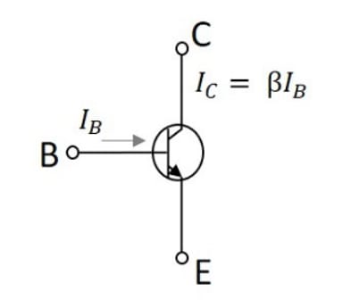
This region lies between saturation and cutoff. The transistor operates in active region when the emitter junction is forward biased and collector junction is reverse biased. In the active state, collector current is times the base current, i.e.,
Where,
-
= collector current
-
= current amplification factor
-
= base current
Saturation region
This is the region in which transistor tends to behave as a closed switch. The transistor has the effect of its collector and Emitter being shorted. The collector and Emitter currents are maximum in this mode of operation. The figure below shows a transistor working in saturation region.
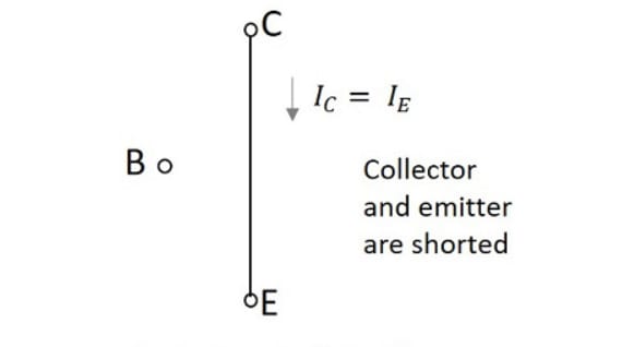
The transistor operates in saturation region when both the emitter and collector junctions are forward biased. As it is understood that, in the saturation region the transistor tends to behave as a closed switch, we can say that,
Where,
- = collector current
- = emitter current
Cutoff region
This is the region in which transistor tends to behave as an open switch. The transistor has the effect of its collector and base being opened. The collector, emitter and base currents are all zero in this mode of operation. The following figure shows a transistor working in cutoff region.
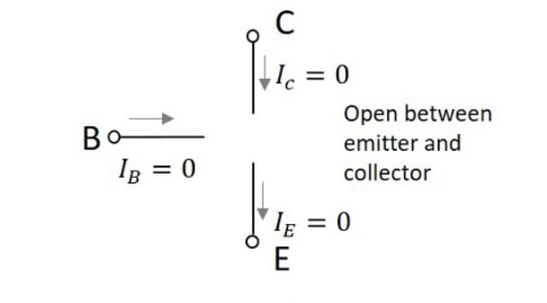
The transistor operates in cutoff region when both the emitter and collector junctions are reverse biased. As in cutoff region, the collector current, emitter current and base currents are nil, we can write as
Where,
- = collector current
- = emitter current
- = base current
Semiconductor Diodes
p- n junction diode , Depletion layer , Energy diagrams of p-n junction and depletion region , Biasing of diode and V-I Characteristics; Rectifiers - half- wave , full- wave and bridge rectifiers; Filters - L , C , LC and π filters ; Zener diode , V-I Characteristics and Zener diode as voltage regulator.
Transistor Biasing
Transistor biasing and bias stabilization, Operating point, Stability factor, Analysis of fixed bias, collector to base bias, Emitter resistance bias circuit and self bias circuit