Semiconductor Diode
A semiconductor diode is a two-terminal electronic device that allows current to flow in one direction while blocking it in the opposite direction. It is made from a p-n junction formed by joining p-type and n-type semiconductor materials.
Operation of a Semiconductor Diode
-
Formation of the p-n Junction:
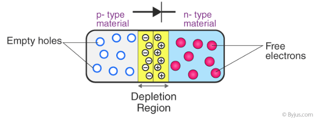
- A diode consists of p-type material (with holes as the majority carriers) and n-type material (with electrons as the majority carriers) joined together.
- When the p-type and n-type materials come into contact, electrons from the n-side diffuse into the p-side, and holes from the p-side diffuse into the n-side.
- This diffusion creates a depletion region around the junction, where free charge carriers are depleted. This region forms an electric field that opposes further movement of electrons and holes.
-
Forward Bias:
- When the positive terminal of a power source is connected to the p-side and the negative terminal to the n-side, the diode is forward-biased.
- The applied voltage reduces the potential barrier of the depletion region, allowing current to flow as electrons from the n-side and holes from the p-side move across the junction.
- Once the forward voltage (typically 0.7V for silicon diodes and 0.3V for germanium diodes) is exceeded, the diode conducts a significant current.
-
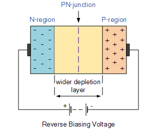
Reverse Bias:
- When the positive terminal is connected to the n-side and the negative terminal to the p-side, the diode is reverse-biased.
- The applied voltage increases the width of the depletion region, creating a larger barrier that prevents current flow.
- Only a very small reverse saturation current flows, caused by minority charge carriers. This current is typically negligible but can increase with temperature.
-
Breakdown:
- If the reverse bias voltage exceeds a certain level (called the breakdown voltage), the diode undergoes avalanche or Zener breakdown (depending on the diode type and doping level).
- During breakdown, the diode conducts a large reverse current, which can damage the diode if it is not designed for such operation (as in Zener diodes).
Characteristics of a Semiconductor Diode
-
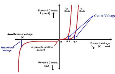
I-V Characteristics:
- The current-voltage (I-V) characteristics of a diode show a sharp distinction between forward and reverse bias operation.
- Forward Bias: Current increases exponentially with applied voltage once the threshold voltage is exceeded.
- Reverse Bias: Current remains very low (reverse saturation current) until the breakdown voltage is reached.
-
Threshold (Cut-in) Voltage:
- This is the minimum forward voltage required for the diode to start conducting significantly (around 0.7V for silicon and 0.3V for germanium diodes).
-
Reverse Saturation Current (Leakage Current):
- A small current flows under reverse bias due to minority carriers. It is typically in the nanoampere range for silicon diodes and increases with temperature.
-
Breakdown Voltage:
- The reverse voltage at which a diode begins to conduct in reverse bias due to breakdown. Diodes are designed to withstand a specific maximum reverse voltage before breakdown occurs.
-
Forward and Reverse Resistance:
- Forward Resistance: When forward-biased, the diode has a low resistance once the threshold voltage is crossed, allowing current to pass easily.
- Reverse Resistance: When reverse-biased, the diode has a very high resistance, effectively blocking current flow.
-
Capacitance:
- Due to the depletion region, diodes exhibit a small capacitance in reverse bias, called junction capacitance. This capacitance decreases as reverse bias increases and is higher in diodes with larger junction areas.
p-n junction Diode
A semiconductor diode is a p-n junction diode consisting of a p-n junction. This junction is formed by joining a p-type semiconductor region, which has an excess of positively charged 'holes', and an n-type semiconductor region, which has an excess of negatively charged electrons. This diode allows current to flow in one direction when forward-biased and blocks current in the opposite direction when reverse-biased. It is a fundamental component in electronics and is widely used for rectification, signal modulation, voltage regulation, and many other applications.
Formation of p-n Junction Diodes
Consider a thin sheet of p-type silicon semiconductor. If a small amount of pentavalent impurity is added, a portion of the p-type silicon will be converted to n-type silicon. This sheet will now consist of both a p-type and an n-type region, with a junction between the two. The formation of a p-n junction involves two main processes: diffusion and drift.
As we know, the concentration of holes and electrons on either side of a junction differs. Holes from the p-side diffuse to the n-side, while electrons from the n-side diffuse to the p-side. This results in a diffusion current flowing across the junction.
Behavior at the Junction:
- When an electron diffuses from the n-side to the p-side, it leaves behind an ionized donor on the n-side, which remains stationary.
- A layer of positive charge develops on the n-side of the junction as this process continues.
- When a hole is transferred from the p-side to the n-side, it leaves behind an ionized acceptor on the p-side, leading to the development of a layer of negative charges on the p-side of the junction.
- The region with positive and negative charges on either side of the junction is known as the depletion region.
- Due to the presence of this positive space charge region on each side of the junction, an electric field is generated from the positive charge to the negative charge. This electric field causes electrons on the p-side of the junction to move towards the n-side. This movement of electrons is termed as drift.
- It is important to note that the drift current flows in the opposite direction to the diffusion current.
Drift Current
- Drift current occurs when charge carriers move in response to an applied electric field within a semiconductor.
- The magnitude of drift current depends on factors such as minority charge carrier concentration, electric field strength, and the mobility of charge carriers. Mobility, influenced by temperature and impurity scattering, affects how easily carriers move in response to the field.
- Higher temperatures generally result in increased thermal energy of charge carriers, potentially leading to higher mobility and thus contributing to higher drift currents.
Diffusion Current
- Diffusion current arises from the movement of charge carriers across a semiconductor due to a concentration gradient, without the need for an external electric field.
- The rate of diffusion current is influenced by factors such as the concentration gradient, diffusion coefficient of charge carriers, and the rate of change of carrier concentration per unit length.
- While it's generally true that higher doping levels can lead to increased diffusion currents due to steeper concentration gradients, excessive doping may also introduce non-ideal behaviors such as increased recombination rates. Therefore, there's a limit to the relationship between doping and diffusion current.
Fermi Level: The Fermi level indicates the energy level at which the probability of finding an electron is 0.5 (50%) at absolute zero temperature. Electrons occupy energy levels below the Fermi level at absolute zero, positioning the Fermi level between the valence and conduction bands.
P-N Junction Formula
where:
- is the zero-bias junction voltage.
- is the thermal voltage at room temperature, which is 26 mV.
- and denote the impurity concentrations.
- denotes the intrinsic concentration.
Applications of P-N Junction Diode
PN junction diodes find numerous applications in the field of electronics. Here are some of their key uses:
- Rectification: One of the most common applications of a PN junction diode is rectification, where it converts alternating current (AC) into direct current (DC).
- Zener Diodes for Voltage Regulation: Zener diodes, a special type of PN junction diode, are employed in circuits for voltage regulation.
- Switching Function: Since diodes conduct current only in forward bias, they serve as switches in electrical circuits. They are used to control the flow of current and toggle certain components on and off within complex circuits.
- Photodiodes: Reverse-biased PN junction diodes are utilized as photodiodes due to their sensitivity to light. They find applications in light detection and sensing devices.
- Light-Emitting Diodes (LEDs): LEDs are another special type of PN junction diode. When forward-biased, they emit light, making them invaluable in lighting applications, displays, and indicators.
Depletion Layer
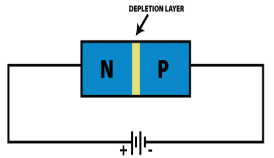
The depletion layer, also referred to as the depletion region or space charge region, is a crucial feature that arises at the junction between a p-type semiconductor and an n-type semiconductor within semiconductor devices like diodes or transistors. This region is characterized by a scarcity or depletion of majority charge carriers (electrons in n-type and holes in p-type), which occurs during the formation of the p-n junction through the diffusion process.
Formation of the Depletion Layer
When the p-type and n-type materials are brought into contact, the behavior of the junction differs from that of the individual materials. Electrons and holes, abundant near the junction, interact due to the Coulombic force between negative electrons and positive holes. Upon the formation of the p-n junction, some electrons from the n-type material diffuse across the junction and combine with holes in the p-type material, resulting in the creation of negative ions in the p-region and positive ions in the n-region. This process leads to the establishment of the depletion layer, serving as a barrier that impedes further electron flow from the n-region to the p-region.
Significance of the Depletion Layer
The depletion layer plays a pivotal role in semiconductor device functionality. By depleting free charge carriers, it generates an electric field and a potential barrier, influencing various aspects such as current flow, capacitance, and device performance. Understanding and managing the depletion layer are essential for optimizing the operation of semiconductor devices.
Energy Diagram of p-n Junction and Depletion Region
The valence and conduction bands in an n-type material are at slightly lower energy levels than the valence and conduction bands in a p-type material. Recall that p-type material has trivalent impurities and n-type material has pentavalent impurities. The trivalent impurities exert lower forces on the outer-shell electrons than the pentavalent impurities. The lower forces in p-type materials mean that the electron orbits are slightly larger and hence have greater energy than the electron orbits in the n-type materials.
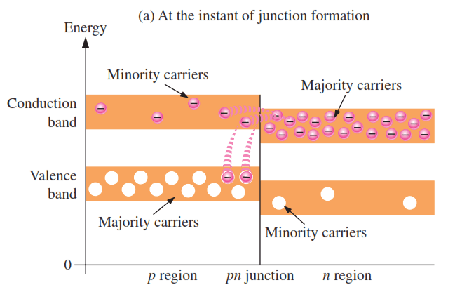
An energy diagram for a pn junction at the instant of formation is shown in Figure (a). As you can see, the valence and conduction bands in the n region are at lower energy levels than those in the p region, but there is a significant amount of overlapping.
The free electrons in the n region that occupy the upper part of the conduction band in terms of their energy can easily diffuse across the junction (they do not have to gain additional energy) and temporarily become free electrons in the lower part of the p-region conduction band. After crossing the junction, the electrons quickly lose energy and fall into the holes in the p-region valence band as indicated in Figure (a).
After crossing the junction, the electrons recombine with holes in the p-region valence band, creating a current flow. This diffusion process continues until an equilibrium is reached. As the diffusion continues, the depletion region begins to form and the energy level of the n-region conduction band decreases. The decrease in the energy level of the conduction band in the n region is due to the loss of the higher energy electrons that have diffused across the junction to the p region. Soon, there are no electrons left in the n-region conduction band with enough energy to get across the junction to the p-region conduction band, as indicated by the alignment of the top of the n-region conduction band and the bottom of the p-region conduction band in Figure (b). At this point, the junction is at equilibrium; and the depletion region is complete because diffusion has ceased. There is an energy gradiant across the depletion region which acts as an “energy hill” that an n-region electron must climb to get to the p region.
Notice that as the energy level of the n-region conduction band has shifted downward, the energy level of the valence band has also shifted downward. It still takes the same amount of energy for a valence electron to become a free electron. In other words, the energy gap between the valence band and the conduction band remains the same.
Biasing Conditions for p-n Junction Diodes
There are two operating regions in the P-N junction diode:
- P-type
- N-type
The voltage applied determines one of three biasing conditions for p-n junction diodes:
- Zero Bias: There is no external voltage applied to the P-N junction diode.There is no external voltage provided to the p-n junction diode while it is at zero bias.
- Forward bias: The p-type is linked to the positive terminal of the voltage source, while the n-type is connected to the negative terminal.
- Reverse bias: The p-type is linked to the negative terminal of the voltage source, while the n-type is connected to the positive terminal.
Forward Biased P-N Junction
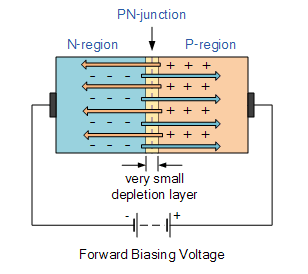
In forward bias condition, the p-type region is connected to the positive terminal and the n-type region to the negative terminal of the external voltage. This reduces the potential barrier at the junction. For silicon diodes, a forward voltage of around 0.7 V significantly reduces the barrier, allowing majority carriers (electrons in n-type and holes in p-type) to diffuse more easily across the junction. This leads to a rapid increase in current flow, resulting in the non-linear behavior observed in the current-voltage (I-V) characteristic curve.
The current through a forward-biased diode can be described by the Shockley diode equation:
where:
- is the diode current,
- is the reverse saturation current (a very small current),
- is the voltage across the diode,
- is the ideality factor (typically between 1 and 2, depending on the diode),
- is the thermal voltage, given by (approximately 26 mV at room temperature),
- is the Boltzmann constant,
- is the absolute temperature in Kelvin,
- is the charge of an electron.
Reverse Biased P-N Junction
When the diode is in reverse bias, the p-type region is connected to the negative terminal and the n-type region to the positive terminal. This widens the potential barrier, making it harder for majority carriers to cross the junction. However, a small reverse saturation current still flows due to thermally generated minority carriers (electrons in p-type and holes in n-type) that can diffuse across the junction in a limited way. As the reverse voltage increases, these minority carriers gain some kinetic energy, but a significant breakdown typically occurs before they can significantly affect the majority carriers. This breakdown can permanently damage the diode.
In reverse bias, the voltage is negative, making the exponential term in the Shockley diode equation very small. This results in a current that is approximately equal to the reverse saturation :
where:
- is the reverse current (very small and negative),
- is the reverse saturation current.
V-I Characteristics of PN Junction Diode
Forward Bias:
- When the PN junction is forward biased, a small reverse saturation current flows until the applied voltage overcomes the potential barrier.
- Upon exceeding the threshold voltage (also known as the forward voltage drop or cut- in voltage), typically 0.3 V for Germanium and 0.7 V for Silicon, the diode conducts current. This voltage is necessary to overcome the potential barrier across the junction.
- As the forward bias voltage increases beyond the threshold, the current through the diode increases exponentially, facilitating the movement of majority charge carriers across the junction. This results in a steep, linear rise in current, resembling that of an ordinary conductor.
Reverse Bias:
- When the PN junction is reverse biased, a very small current, known as the reverse saturation current, flows due to thermally generated minority charge carriers.
- As the reverse bias voltage (also known as the reverse potential barrier) increases, minority charge carriers gain kinetic energy, enabling some to cross the junction.
- In the phenomenon known as avalanche breakdown, occurring at a certain critical voltage called the breakdown voltage, the accelerated minority charge carriers collide with semiconductor atoms in the depletion region, causing impact ionization. This leads to the generation of additional free charge carriers, resulting in a sharp increase in current through the diode.
- Under reverse bias conditions, the current through the diode remains extremely small, typically in the range of microamperes, primarily due to the movement of minority charge carriers.
Rectifiers
The process in which alternating voltage or alternating current is converted into direct voltage or direct current is known as rectification. In our country domestic supply has a voltage 220V varying at a frequency 50Hz. For operating most of the electronic equipment, dc voltage is required. Hence it is necessary to convert ac voltage of main power supply to dc voltage. The device used for this conversion process is called as rectifier. The junction diode has the property of offering low resistance and allowing current to flow through it in the forward biased condition. This property is used in the process of rectification.
A PN junction diode can be used as:
- Half wave rectifier
- Full wave rectifier
- Bridge rectifier.
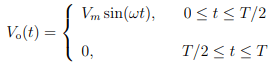
Half Wave Rectifier
It is not a single video but a playlist, and it contains 4 videos. When one video finishes, the next will play automatically.
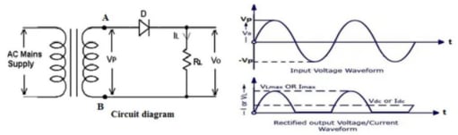
A half-wave rectifier is a circuit that converts an alternating current (AC) signal into a pulsating direct current (DC) signal using a single p-n junction diode, as shown in the figure above.
In a half-wave rectifier circuit, an alternating voltage is applied to a single diode connected in series with a load resistor (). An AC signal consists of both positive and negative half cycles. The p-n junction diode conducts only during the positive half cycle of the input AC cycle.
-
Positive Half Cycle: During the positive half cycle, the diode (D) is forward biased (anode positive, cathode negative) and conducts current () that flows through the load resistor (). Since the diode offers low resistance, a significant current flows in this direction. This current flow results in a voltage () appearing across , replicating the positive half wave of the input voltage at the output (minus a small voltage drop across the diode).
-
Negative Half Cycle: During the negative half cycle, the diode (D) is reverse biased (anode negative, cathode positive) and does not conduct. Consequently, no current flows through the load resistor (), and there is no output voltage (). This means the negative half cycle of the input voltage is not utilized.
Overall, the half-wave rectifier produces a pulsating DC voltage with a ripple voltage component because it only utilizes half of the AC waveform.
Half Wave Rectifier Formulas
Alternating Current (AC)
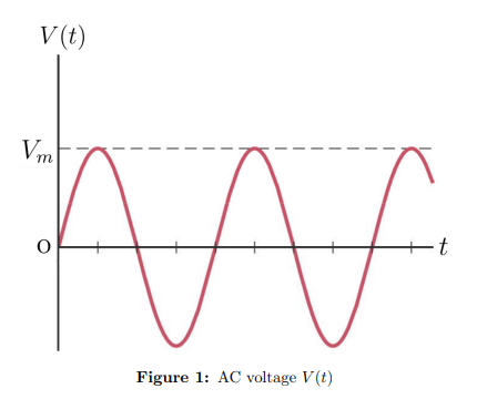
Alternating current (AC) describes the flow of charge that changes direction periodically. As a result, the voltage level also reverses along with the current. AC is used to deliver power to houses, office buildings, etc. The AC voltage of a periodic waveform may be written as
where is the angular frequency of the waveform or voltage and T is the time period of the voltage and represents the maximum or peak value of the alternating current (AC) voltage waveform. This is often referred to as the amplitude of the waveform. It indicates the maximum positive or negative value that the voltage reaches during each cycle of the AC waveform.
-
Average voltage over the time period
The average value of V(t) over the time period T is defined as
Hence,

Therefore, the average value of an AC voltage over the time period of the oscillation is zero.
-
Average voltage over half of the time period
Since the average value of the AC voltage over the time period is zero, we may calculate the average value over the half of the time period using a similar definition as (1). Therefore,

-
The RMS value of the AC voltage
The term ”RMS” stands for ”Root-Mean-Squared”, also called the effective or heating value of alternating current, is equivalent to a DC voltage that would provide the same amount of heat generation in a resistor as the AC voltage would if applied to that same resistor. RMS is not an ”Average” voltage, and its mathematical relationship to peak voltage varies depending on the type of waveform. The RMS value is the square root of the mean (average) value of the squared function of the instantaneous values. For the voltage V (t) given in (1) it can be written as
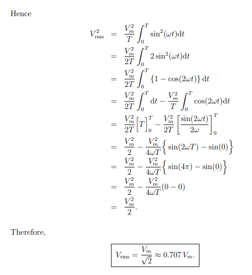
Important relations to remember
A few handy things to keep in mind about RMS values that apply when dealing with a sine wave, are as follows:
- ≈ 0.707 x peak AC voltage = 70.7 % of peak voltage
- Peak AC voltage ≈ 1.414 x = 141.1 % of
- ≈ 0.637 x peak AC voltage = 63.7 % of peak voltage
Therefore, An AC voltage given by (1), the output voltage of a half wave rectifier will be (for an ideal diode)
-
Average output voltage of a half wave rectifier
To calculate the average voltage, Vdc, of the pulsating DC output of a half wave rectifier we use the definition (1). Therefore, for the voltage (4) we have

Hence, Avg output voltage of half wave rectifier is =
-
RMS value of the output voltage of a half wave rectifier
To calculate the RMS value of the output voltage, Vrms, of the pulsating DC output of a half wave rectifier we use the definition (3). Therefore, for the voltage (4) we have

Hence, RMS value of the output voltage of half wave rectifier is =
-
Ripple factor of half wave rectifier
Ripple is the unwanted AC component remaining when converting the AC voltage waveform into a DC waveform. Even though we try out best to remove all AC components, there is still some small amount left on the output side which pulsates the DC waveform. This undesirable AC component is called ripple. To quantify how well the half wave rectifier can convert the AC voltage into DC voltage, we use what is known as the ripple factor (represented by γ). The ripple factor is the ratio between the RMS value of the AC voltage and the DC voltage of the rectifier.

Note that the RMS value of the AC component of the signal is and is the RMS value of the whole voltage signal.
To calculate , the RMS value of the AC component present in the output of the half wave rectifier we write the output voltage as,
where is the AC component remaining when converting the AC voltage waveform into a DC waveform. The RMS value of the AC component present in the output of the half wave rectifier is given by,

Using the values of and given in 5 and 6 respectively for the half wave rectifier we find the the ripple factor as,

Note that to construct a good rectifier, one should keep the ripple factor as low as possible. This is why capacitors and inductors as filters are used to reduce the ripples in the circuit.
-
Efficiency of half wave rectifier
The ratio of the DC power available at the load to the applied input AC power is known as the efficiency, η. Mathematically it can be given as:
and
This indicates that the half wave rectifier can convert maximum 40.53% of AC power into DC power, and the remaining power of 59.47% is lost in the rectifier circuit. In fact, 50% power in the negative half cycle is not converted and the remaining 9.47% is lost in the circuit.
-
Form factor of half wave rectifier
Form factor (f.f.) is defined as the ratio between RMS load voltage and average load voltage. The form factor of the half wave rectifier is as,

The form factor is used to get the information of the waveform.
-
Peak Inverse Voltage (PIV) of half wave rectifier
Peak Inverse Voltage (PIV) is the maximum voltage that the diode can withstand during reverse bias condition. If a voltage is applied more than the PIV, the diode will be destroyed. The peak-inverse-voltage (PIV) rating of a diode is of the primary importance in the design of rectification systems. During negative half cycles of the input voltage, the diode is reversed biased, no current flows through the load resistance and so causes no voltage drop across load resistance and consequently the whole of the input voltage appears across the diode. Thus the maximum voltage, that appears across the diode, is equal to the peak value of the secondary voltage i.e. . Thus for a half-wave rectifier
PIV =
-
Peak factor of half wave rectifier
It is defined as the ratio of the peak value of the output voltage to the RMS value of the output voltage. The peak factor of the half wave rectifier is as,
Peak factor =
To learn about formulas for other terms such as load current and Transformer Utilization Factor (TUF), please refer to the playlist provided above on the topic of half-wave rectifiers.
Advantages of Half Wave Rectifier
- The half wave rectifier circuit is simple and easy to implement, requiring only one diode and a load resistor.
- Due to its simplicity, the components required for a half wave rectifier are inexpensive, making it cost-effective for various applications.
- It is well-suited for low power applications where only a small amount of DC voltage is required, such as in signal detection circuits.
- Half wave rectifiers are commonly used in battery chargers to convert AC voltage to DC voltage for charging batteries.
- Its simple construction and low component count contribute to a lightweight design, making it suitable for portable electronic devices.
Disadvantages of Half Wave Rectifier
- Half wave rectifiers have low efficiency because they utilize only half of the input AC waveform, wasting the other half as heat.
- The output of a half wave rectifier is a pulsating DC voltage, which may not be suitable for applications requiring a steady DC voltage.
- The pulsating nature of the output voltage results in a high ripple factor, leading to undesirable fluctuations in the output voltage.
- The output voltage of a half wave rectifier is less than the peak voltage of the input AC signal, limiting its applicability in high voltage applications.
- The diode used in a half wave rectifier is subjected to high voltage and current stresses during operation, potentially leading to premature failure if not properly rated.
Application of Half Wave Rectifier
- The half wave rectifier is used in battery chargers where the input AC voltage is converted into DC voltage to charge the battery.
- The half wave rectifier is used in small power supplies where low DC voltage is required for electronic devices.
- The half wave rectifier is used in signal detectors to extract the envelope of an AM (amplitude-modulated) signal.
- The half wave rectifier can be used in LED lighting circuits where the input AC voltage is rectified to provide DC voltage to the LEDs.
- The half wave rectifier is used in radio receivers to extract the audio signal from the modulated radio frequency carrier.
- The half wave rectifier is used in temperature sensors to rectify the output of a thermocouple to obtain a measurable DC voltage.
Full Wave Rectifier
It is not a single video but a playlist, and it contains 2 videos. When one video finishes, the next will play automatically.
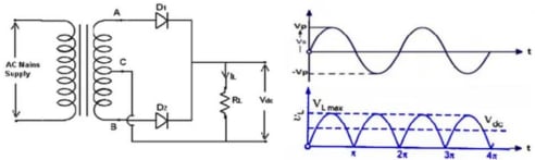
A full-wave rectifier is a circuit designed to convert an AC signal into a DC signal using two p-n junction diodes, as illustrated in the figure above. Unlike a half-wave rectifier, it utilizes both positive and negative half cycles of the input AC voltage, resulting in a more efficient rectification process.
In a full-wave rectifier circuit, a center-tapped transformer provides the input AC voltage. The center tap creates two identical secondary winding halves with a common center point. The two diodes ( and ) are connected with their cathodes (negative terminals) joined to the center tap, and their anodes (positive terminals) connected to each end of the secondary winding, respectively.
-
Positive Half Cycle: During the positive half cycle of the secondary voltage, diode is forward biased (anode positive, cathode negative) and conducts current. This current flows through the load resistor () and the upper half of the secondary winding. As a result, an output voltage () is developed across in the same direction as the positive half cycle of the input voltage (minus a small voltage drop across the diode). Meanwhile, diode is reverse biased and does not conduct.
-
Negative Half Cycle: During the negative half cycle of the secondary voltage, diode becomes forward biased and conducts. Current flows through and the lower half of the secondary winding, again generating an output voltage () across in the same direction (positive) due to the current flow direction. During this half cycle, diode is reverse biased.
Key Points:
- Notably, the direction of current flow through the load resistor () remains the same during both half cycles due to the way the diodes are connected. This ensures a more continuous, rectified output voltage compared to a half-wave rectifier.
- By utilizing both positive and negative half cycles of the input waveform, the full-wave rectifier achieves higher efficiency compared to a half-wave rectifier. -Although significantly improved compared to a half-wave rectifier, the output voltage from a full-wave rectifier with a center-tapped transformer still contains some ripple voltage. This can be further reduced using filters in the circuit.
Alternative Full-Wave Rectification (Bridge Rectifier):
It's important to note that a different type of full-wave rectifier, called a bridge rectifier, can achieve full-wave rectification without requiring a center-tapped transformer. The bridge rectifier uses four diodes in a specific configuration to achieve the same result.
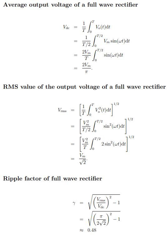
Full Wave Rectifier Formulas
For an AC voltage given by (1) the waveform of the output voltage of a full wave rectifier can be written as (for an ideal diode),
Efficiency of full wave rectifier
and
Form factor of full wave rectifier
Form Factor =
Peak Inverse Voltage (PIV) of full wave rectifier
Peak inverse voltage(PIV) or peak reverse voltage(PRV) can be defined as the maximum value of the reverse voltage of a diode, which occurs at the peak of the input cycle when the diode is in reverse bias.
PIV of center tapped full wave rectifier is .
Peak factor of full wave rectifier
Peak factor =
To learn about formulas for other terms such as load current and Transformer Utilization Factor (TUF), please refer to the playlist provided above on the topic of full-wave rectifiers.
Advantages of Full Wave Rectifier
- Compared to a half-wave rectifier, a full-wave rectifier utilizes both halves of the input AC waveform, resulting in higher efficiency.
- The output of a full-wave rectifier has less ripple compared to a half-wave rectifier, making it more suitable for applications requiring a smoother DC voltage.
- The output voltage of a full-wave rectifier is higher than that of a half-wave rectifier for the same input AC voltage, making it suitable for applications requiring higher DC voltage levels.
- A full-wave rectifier utilizes both positive and negative half cycles of the input AC waveform, leading to a more continuous and consistent output.
Disadvantages of Full Wave Rectifier
- A full-wave rectifier circuit is more complex and requires more components compared to a half-wave rectifier, making it slightly more expensive and difficult to implement.
- Due to the additional components required, the cost of a full-wave rectifier circuit may be higher than that of a half-wave rectifier.
Applications of Full Wave Rectifier
- Full-wave rectifiers are commonly used in power supply circuits to convert AC voltage from mains power into DC voltage for electronic devices.
- Full-wave rectifiers are used in battery chargers to efficiently convert AC voltage to DC voltage for charging batteries.
- Full-wave rectifiers are used in motor speed control circuits to convert AC voltage to DC voltage for controlling the speed of motors.
- Full-wave rectifiers are used in audio amplifier circuits to convert AC voltage from audio sources into DC voltage for amplification.
- Full-wave rectifiers are used in lighting systems, such as LED drivers, to convert AC voltage to DC voltage for powering LEDs.
A comparison of different parameters related to the half and full wave rectifiers are given below:
| Parameters | Half wave rectifier | Full wave rectifier |
|---|---|---|
| Number of diodes | 1 | 2 or 4 |
| Maximum efficiency | 40.53% | 81.06% |
| Peak inverse voltage | ||
| Average voltage (no load) | ||
| (no load) | ||
| Ripple Factor | 1.21 | 0.48 |
| Form Factor | 1.57 | 1.11 |
| Output Frequency | f | 2f |
Bridge Rectifier
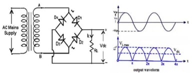
The bridge rectifier employs four individual rectifying diodes arranged in a closed-loop "bridge" configuration, eliminating the need for a special center-tapped transformer. This configuration not only reduces size and cost but also enhances efficiency and performance compared to traditional rectification methods.
In the bridge rectifier circuit, the single secondary winding of the transformer is connected across the input terminals of the bridge network, while the load () is connected across the output terminals. The four diodes, labeled to , are arranged in series pairs, with only two diodes conducting current during each half cycle.
During the positive half cycle of the input supply voltage, diodes and conduct in series, allowing current to flow through the load (). Conversely, diodes and are reverse biased and remain non-conductive.
During the negative half cycle, diodes and conduct in series, while and are reverse biased. Again, the current flows through the load () in the same direction as during the positive half cycle.
Since the current through the load is unidirectional, the voltage developed across the load is also unidirectional, resulting in a smoother and continuous DC output similar to that of a two-diode full-wave rectifier.
Bridge Rectifier Formulas
- Efficiency (η): Both bridge and full-wave rectifiers with a center-tapped transformer achieve a similar efficiency of around 81.06%. This is because they utilize both positive and negative halves of the AC waveform.
- Form Factor (ff): The form factor for both rectifier types is approximately 1.11, indicating a relatively smooth DC output compared to a half-wave rectifier.
- Peak Factor: The peak factor for both bridge and full-wave rectifiers is around , suggesting some residual ripple voltage in the output.
- Peak Inverse Voltage (PIV): This is a crucial difference. In a bridge rectifier, the PIV for each diode is equal to the peak voltage () of the AC input signal. In a full-wave rectifier with a center-tapped transformer, the PIV for each diode is twice the peak voltage () because the entire secondary voltage appears across a single diode during the reverse bias condition.
To learn about formulas for other terms, please refer to the video above on the topic of bridge rectifier.
Advantages of Bridge Rectifier
- Bridge rectifiers achieve a maximum efficiency of around 81.06%. This is because they utilize both positive and negative half cycles of the AC input signal, resulting in less power wasted compared to half-wave rectifiers.
- The bridge rectifier produces a rectified DC output with less ripple voltage compared to a half-wave rectifier. This is because both positive and negative halves of the AC waveform are rectified in the same direction.
- Unlike full-wave rectifiers using a center-tapped transformer, bridge rectifiers only require a single secondary winding transformer. This simplifies the circuit design and reduces cost.
- Bridge rectifiers can handle a wide range of AC voltages, making them suitable for various applications.
- Bridge rectifiers are typically constructed with four small diodes in a compact bridge configuration, leading to a smaller footprint compared to some full-wave rectifier circuits.
Disadvantages of Bridge Rectifier
- There is a small voltage drop across each diode in the bridge rectifier due to the forward bias current. This can slightly reduce the output DC voltage compared to the ideal case.
- The forward bias current through the diodes also generates some heat dissipation. This may need to be considered in high-power applications.
- Compared to a half-wave rectifier (one diode), a bridge rectifier uses four diodes. This can slightly increase the cost and component complexity.
Applications of Bridge Rectifier
Bridge rectifiers are extensively used in various electronic circuits due to their efficiency, versatility, and compact size. Here are some common applications:
- Bridge rectifiers are an essential component in power supplies, converting AC mains voltage from the wall outlet into DC voltage to power electronic devices.
- They play a crucial role in battery chargers, rectifying AC voltage to DC voltage for charging batteries.
- Bridge rectifiers are used in motor speed control circuits to convert AC voltage to DC voltage, allowing for control over motor speed.
- In audio amplifier circuits, bridge rectifiers convert AC voltage from audio sources into DC voltage for amplification.
- Bridge rectifiers are used in LED driver circuits to convert AC voltage to DC voltage for powering LEDs.
- They are employed in solar power systems to convert the DC output from solar panels into DC voltage suitable for battery storage or grid connection (often with additional power conversion stages).
Filters
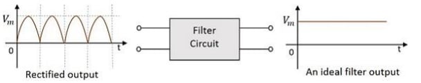
The rectifier converts the Alternating Current (AC) into Direct Current (DC). But the obtained Direct Current (DC) at the output is not a pure Direct Current (DC). It is a pulsating Direct Current (DC). The pulsating Direct Current (DC) is not constant. It fluctuates with respect to time. When this fluctuating Direct Current (DC) is applied to any electronic device, the device may not work properly. Sometimes the device may also be damaged. So the fluctuating Direct Current (DC) is not useful in most of the applications. Therefore, we need a Direct Current (DC) that does not fluctuate with respect to time. The only solution for this is smoothing the fluctuating Direct Current (DC). This can be achieved by using a device called filter. A filter circuit is an electronic device which blocks the ac component present in the rectified output and allows the dc component to reach the load. The following figure shows the functionality of a filter circuit.
A filter circuit is constructed using two main components, inductor and capacitor:
- An inductor allows dc and blocks ac.
- A capacitor allows ac and blocks dc
Types of Filters
Series Inductor Filter or L Filter
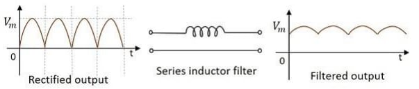
As an inductor allows dc and blocks ac, a filter called Series Inductor Filter can be constructed by connecting the inductor in series, between the rectifier and the load. The figure above shows the circuit of a series inductor filter.
The rectified output when passed through this filter, the inductor blocks the ac components that are present in the signal, in order to provide a pure dc. This is a simple primary filter.
Shunt Capacitor Filter or C Filter
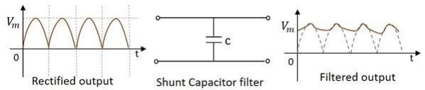
As a capacitor allows ac through it and blocks dc, a filter called Shunt Capacitor Filter can be constructed using a capacitor, connected in shunt, as shown in the following figure.
The rectified output when passed through this filter, the ac components present in the signal are grounded through the capacitor which allows ac components. The remaining dc components present in the signal are collected at the output.
The above filter types discussed are constructed using an inductor or a capacitor. Now, let's try to use both of them to make a better filter. These are combinational filters.
L-C Filter
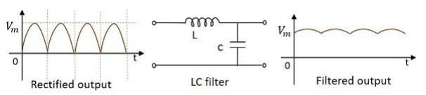
A filter circuit can be constructed using both inductor and capacitor in order to obtain a better output where the efficiencies of both inductor and capacitor can be used. The figure above shows the circuit diagram of a LC filter.
The rectified output when given to this circuit, the inductor allows dc components to pass through it, blocking the ac components in the signal. Now, from that signal, few more ac components if any present are grounded so that we get a pure dc output.
This filter is also called as a Choke Input Filter as the input signal first enters the inductor. The output of this filter is a better one than the previous ones.
Pi Filter
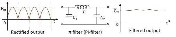
This is another type of filter circuit which is very commonly used. It has capacitor at its input and hence it is also called as a Capacitor Input Filter. Here, two capacitors and one inductor are connected in the form of π shaped network. A capacitor in parallel, then an inductor in series, followed by another capacitor in parallel makes this circuit. If needed, several identical sections can also be added to this, according to the requirement. The figure above shows a circuit for π filter or Pi-filter.
Working of a Pi filter: In this circuit, we have a capacitor in parallel, then an inductor in series, followed by another capacitor in parallel.
- Capacitor - This filter capacitor offers high reactance to dc and low reactance to ac signal. After grounding the ac components present in the signal, the signal passes to the inductor for further filtration.
- Inductor L - This inductor offers low reactance to dc components, while blocking the ac components if any got managed to pass, through the capacitor .
- Capacitor - Now the signal is further smoothened using this capacitor so that it allows any ac component present in the signal, which the inductor has failed to block.
Zener Diode
A Zener diode is a type of semiconductor diode specifically designed to operate in the reverse-biased or breakdown region. This breakdown behavior makes them valuable components for voltage regulation and protection in electronic circuits.
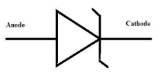
Zener Diode Symbol
The symbol for Zener diode is represented as below,
Zener Diode Circuit
We can define Zener diode as a single diode connected in a reverse bias. It can be connected in reverse bias positive as in the circuit shown below,
Working of Zener Diode
When a Zener diode is forward-biased (anode positive with respect to cathode), it behaves like a normal diode, allowing current to flow. However, in the reverse-biased condition (cathode positive than anode), a unique phenomenon occurs. As the reverse voltage increases, the depletion region around the p-n junction widens. When this reverse voltage reaches a specific value, known as the Zener breakdown voltage (), a sudden and significant increase in reverse current occurs. This breakdown allows substantial current to flow in the reverse direction.
There are two primary mechanisms that contribute to Zener breakdown:
-
Zener Breakdown (Quantum Tunneling): This effect is dominant at lower breakdown voltages (typically up to 5.6 volts). Under high electric field strength in the depletion region, valence band electrons from the p-type region can tunnel directly through the bandgap to the conduction band of the n-type region. This tunneling current creates the breakdown phenomenon.
-
Avalanche Breakdown: This effect becomes more prominent at higher breakdown voltages (above 5.6 volts). In avalanche breakdown, strong electric fields within the depletion region accelerate free electrons to very high velocities. These energetic electrons collide with other atoms in the crystal lattice, knocking out additional electrons. The newly created electrons are also accelerated by the electric field, further colliding with atoms and generating even more electrons. This creates a snowball effect, leading to a rapid increase in reverse current.
The relative contributions of Zener breakdown and avalanche breakdown depend on the doping levels of the p and n regions and the applied voltage. In most practical Zener diodes, both effects contribute to the overall breakdown phenomenon.
| Feature | Zener Breakdown | Avalanche Breakdown |
|---|---|---|
| Primary Mechanism | Zener effect (Quantum tunneling) | Impact ionization (Avalanche effect) |
| Typical Voltage Range | More likely to occur at lower voltages | More likely to occur at higher voltages |
| Doping Levels | More prominent at lower doping levels | More significant at higher doping levels |
| Electric Field Strength | Strong electric field causing electron tunneling | Strong electric fields accelerating electrons |
| Velocity of Electrons | Electrons tunnel through the bandgap | Electrons gain high velocities due to acceleration |
| Contribution to Breakdown | Breakdown at lower voltages | Breakdown at higher voltages |
V-I Characteristics of Zener Diode
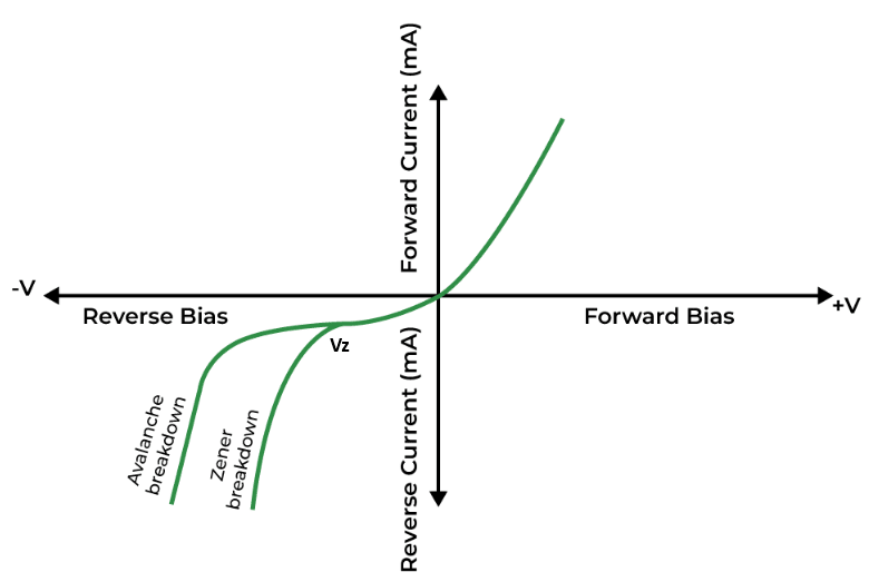
Forward Bias:
In the forward bias region, the zener diode behaves like a regular diode.
Reverse Bias:
In the reverse bias region, a small leakage current flows in the opposite direction until the voltage reaches the breakdown voltage (Vz), which is a characteristic of the specific zener diode.
Breakdown Region:
Beyond the breakdown voltage (Vz), the current through the zener diode increases dramatically with a relatively small increase in voltage. This is because the strong electric field in the depletion region of the diode causes covalent bonds to break, allowing a surge of current. There are two mechanisms for breakdown that can occur in this region:
- Zener breakdown: This typically occurs in more heavily doped zener diodes (doping refers to the addition of impurities to a semiconductor). In this case, the electric field creates enough force to ionize atoms within the depletion region, and the resulting free electrons and holes conduct current.
- Avalanche breakdown: This typically occurs in less heavily doped zener diodes. In this case, the electric field accelerates free electrons in the depletion region to a high enough velocity that they can knock valence electrons out of bound from atoms, creating additional electron-hole pairs. The newly created free electrons are also accelerated by the electric field, further creating more electron-hole pairs in an avalanche effect, resulting in a surge in current.
Operating Region
For zener diodes, the region of interest for operation is in the reverse bias region, beyond the breakdown voltage (Vz). In this region, the zener diode exhibits a nearly constant voltage across the diode, even with significant changes in current. This makes zener diodes useful in voltage regulation applications, where they can be used to provide a stable voltage reference in a circuit.
Application of Zener Diode
- Zener diode is used as a voltage regulator.
- Zener diode is used as a peak clipper in wave shaping circuits.
- Zener diode is used as a fixed reference voltage in transistor biasing circuits.
- Zener diode is used for meter protection against damage from accidental application of excessive voltages.
Zener Diode as a Voltage Regulator
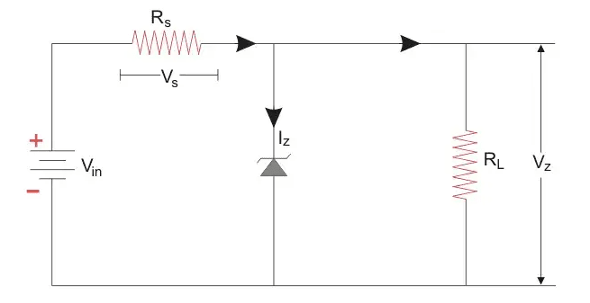
A Zener diode is a specially designed diode that operates effectively in reverse bias conditions. Due to heavier doping, they have a narrower depletion region compared to regular diodes. While regular diodes can be damaged when the voltage across them exceeds the reverse breakdown voltage, Zener diodes are designed to function in this breakdown region. The depletion region in a Zener diode returns to its normal state when the reverse voltage is removed. This unique property of Zener diodes makes them valuable for voltage regulation applications.
The exciting aspect of Zener diodes is that we can select one with a breakdown voltage suitable for our circuit's voltage regulation needs. In the diagram, the Zener diode is connected across the load . Our goal is to regulate the voltage across the load without exceeding the value of . Depending on our requirements, we choose a Zener diode with a breakdown voltage close to the desired voltage across the load. The Zener diode is connected in reverse bias. When the voltage across the diode exceeds the Zener breakdown voltage, a significant current flows through it. As the load is in parallel with the diode, the voltage drop across the load equals the Zener breakdown voltage. Thus, the Zener diode provides a current path, protecting the load from excessive currents. Consequently, the Zener diode serves dual purposes: as a voltage regulator and as a safeguard against excessive current for the load.
A series resistor () is typically included in Zener diode regulator circuits. This resistor limits the current flowing through the Zener diode, preventing it from exceeding its power rating and burning out.
Semiconductors
Energy band concept of materials , difference between metal, insulator and semiconductor , Intrinsic and extrinsic semiconductors (n- type & p- type) , current conduction in semiconductor , Photodiode , photo-transistor , LED and seven- segment display
Bipolar Junction Transistors
Transistor operation and current components in p- n- p and n- p- n transistors , input/output characteristics of CB and CE configurations,Transistor as an Amplifier ,transistor cutoff , saturation and active regions