Semiconductor
A semiconductor is a material that exhibits electrical conductivity between that of a conductor and an insulator. Unlike conductors, which readily allow the flow of electric current, and insulators, which resist it, semiconductors' conductivity can be controlled by factors such as temperature, impurities, or an applied electric field. Semiconductors serve as the foundational components in modern electronics and technology, forming the basis of devices such as diodes, transistors, and integrated circuits. They are typically composed of elements such as silicon, germanium, or compounds like gallium arsenide. The unique electrical properties of semiconductors enable precise control of electrical signals, making them essential for a wide range of electronic systems including computers, smartphones, solar cells, LED lighting, power electronics, sensors, and more.
Why Semiconductors are Important?
Semiconductors are essential because they enable precise control and management of electric current in electronic equipment and devices. Their ability to modulate conductivity allows for the creation of electronic components crucial for processing information, saving energy, and supporting renewable energy technologies such as solar cells. Moreover, semiconductors play a pivotal role in the advancement of various electronic applications, ranging from consumer electronics like computers and smartphones to industrial applications like power electronics and sensor technologies.
What is Energy Band?
In a crystal structure, atoms are closely packed, and electrons interact within this arrangement. Changes in energy levels occur within the electron shells due to these interactions. The energy band concept describes the stable energy states of electrons within different ranges. It illustrates the fluctuation of energy levels in conduction and valence bands.
Energy Band Theory
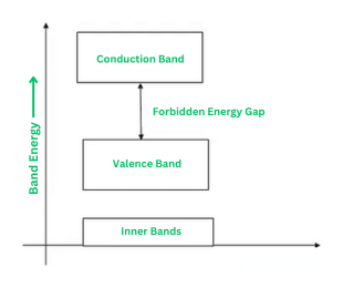
Building upon Bohr's atomic model, which suggests discrete energy levels for each shell of an atom, the energy band theory explains the movement of electrons between inner and outer shells. According to this theory, energy bands are categorized into three types:
- Valence Band
- Forbidden Energy Gap
- Conduction Band
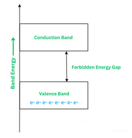
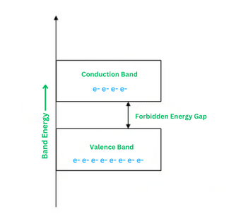
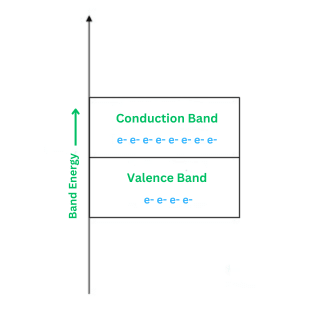
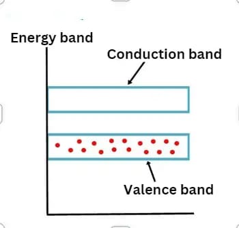
Valence Band
The outermost shell of an atom contains electrons known as valence electrons. These valence electrons occupy a range of energy levels, forming what is called the valence band. The valence band represents the highest energy levels that electrons occupy within the atom in the absence of an external electric field.
Forbidden Energy Gap
The region between the valence and conduction bands, known as the forbidden gap, lacks energy. Electrons can occupy this band but cannot move freely within it, making it inacessible for electrical conduction. A wider band gap indicates weaker binding of electrons to the nucleus within the valence band. To promote electrons from valence band to conduction band, an external force equivalent to the energy of the band gap is required.
Conduction Band
Valence electrons are not strongly bound to the nucleus, allowing some to break free from the outermost orbit even at room temperature. These liberated electrons, known as free electrons or conduction electrons, are responsible for conducting electric current in materials. The conduction band comprises these mobile electrons and is characterized by higher energy levels compared to the valence band.
Difference in Tabular Form
| Property | Valence Band | Forbidden Band (Band Gap) | Conduction Band |
|---|---|---|---|
| Definition | The energy band where electrons are bound to atoms and participate in bonding. | The energy gap between the valence band and conduction band, where no electron states exist. | The energy band where electrons are free to move, allowing electrical conduction. |
| Electron Availability | Contains electrons that are bound to atoms and generally not free to move. | Contains no electrons, as no permissible energy states exist here. | Contains electrons that have gained enough energy to escape atomic bonds, allowing free movement. |
| Energy Level | Lower energy compared to the conduction band. | An intermediate energy range with no available electron states. | Higher energy compared to the valence band. |
| Electron Movement | Electrons here are bound to atoms and cannot move freely across the material. | Electrons cannot exist here, as it is an energy range forbidden for electron occupancy in ideal conditions. | Electrons are free to move throughout the material, enabling conductivity. |
| Holes (Positive Charge Carriers) | When an electron leaves the valence band, a hole is created here, acting as a positive charge carrier. | No holes are present, as it is an unoccupied energy range. | Holes are not present; only electrons exist here. |
| Effect of Temperature | With increased temperature, some electrons in the valence band gain enough energy to jump across the forbidden band to the conduction band. | Higher temperatures or photon energy can enable electron transitions across this band gap. | Higher temperatures promote more electrons into the conduction band, increasing conductivity in semiconductors. |
| Effect of Doping | Doping with acceptors (p-type) creates holes here, enhancing conductivity by hole movement. | Doping can add energy states just below or above the band gap, reducing its effective width and making electron transitions easier. | Doping with donors (n-type) adds electrons close to or within the conduction band, enhancing conductivity. |
| Electron Mobility | Low, as electrons are bound to atoms and have limited mobility. | Not applicable, as electrons do not occupy this range under normal conditions. | High, as electrons are free to move and respond to an electric field. |
| Position in Energy Diagram | Located below the conduction band. | Located between the valence band and conduction band in insulators and semiconductors. | Located above the valence band and separated by an energy gap in semiconductors and insulators. |
Energy Band Influencing Electrical Conductivity
Semiconductors have unique energy bands—specifically, the valence band and the conduction band—that govern electron movement within the material, thereby influencing its conductivity.
-
Energy Band Gap: The energy band gap (Eg) is the energy difference between the valence band (where electrons are bound to atoms) and the conduction band (where electrons are free to move and conduct electricity). In semiconductors, this gap is relatively small, typically between 0.1 eV and 2 eV.
- Small Band Gap: A smaller band gap in semiconductors allows electrons to more easily gain the energy (from thermal excitation or doping) needed to jump from the valence band to the conduction band.
- Electrical Conductivity: When electrons transition into the conduction band, they are free to move and conduct electric current. The smaller the band gap, the more readily electrons can be excited to the conduction band, increasing conductivity.
-
Temperature Influence: Due to the small band gap, semiconductors show a unique relationship between temperature and conductivity:
- Increasing Temperature: As temperature rises, more electrons gain sufficient thermal energy to cross the band gap from the valence band to the conduction band.
- Enhanced Conductivity: With more electrons entering the conduction band at higher temperatures, the electrical conductivity of semiconductors increases. This is in contrast to metals, where conductivity generally decreases with temperature due to increased scattering.
-
Role of Intrinsic and Extrinsic Charge Carriers: In semiconductors, conductivity depends on both intrinsic (native) and extrinsic (doped) charge carriers:
- Intrinsic Carriers: In pure (intrinsic) semiconductors, conductivity is achieved when thermal energy excites electrons from the valence band to the conduction band, leaving behind "holes" in the valence band. These holes act as positive charge carriers, contributing to conductivity along with electrons.
- Extrinsic Carriers: Doping a semiconductor with impurities adds either extra electrons (n-type) or extra holes (p-type), significantly increasing the number of charge carriers in the conduction or valence band, respectively, and thereby enhancing conductivity.
-
Influence of Doping: Doping modifies the energy band structure by introducing impurity atoms into the semiconductor material:
- Donor Levels (n-type): Adding donor atoms (such as phosphorus in silicon) creates energy levels just below the conduction band. These donor electrons require minimal energy to jump into the conduction band, thereby increasing conductivity.
- Acceptor Levels (p-type): Adding acceptor atoms (such as boron in silicon) creates energy levels just above the valence band. Electrons from the valence band can move to these acceptor levels, generating holes that also increase conductivity.
Types of Energy Bands
The energy bands are classified into three types namely:-
- Insulators
- Semiconductors
- Conductor
Insulators
The best examples of insulators are wood and glass. These materials do not permit the flow of electricity through them. Insulators have extremely low conductivity and high resistivity. In an insulator, the energy gap is extremely high, approximately 7 eV. Due to this large energy gap, electrons cannot flow from the valence band to the conduction band, making electrical conduction unfeasible.
Semiconductors
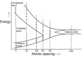
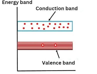
The best examples of semiconductors are Silicon (Si) and Germanium (Ge), which are commonly used materials. The electrical properties of these materials lie between those of conductors and insulators. The following image show the energy band diagrams of semiconductors where the conduction band can be vacant while the valence band is completely filled; however, the forbidden gap between these bands is small, typically around 1 eV. The forbidden gap of Germanium is approximately 0.72 eV, while that of Silicon is around 1.1 eV. Consequently, semiconductors exhibit moderate conductivity. As the temperature of a semiconductor increases, its resistivity increases, leading to decrease in conductivity.
Conductors
A conductor is a type of material where the prohibited energy gap disappears, and the valence band and conduction band become extremely close, partially overlapping. Examples of conductors include Gold, Aluminum, Copper, and Silver. These materials have a high availability of free electrons at room temperature.
The main characteristics of conductors include the absence of a forbidden energy gap, overlapping of the valence and conduction bands, and ample availability of free electrons for conduction. Conductivity increases with the application of even small voltages.
Difference Between Metal, Insulator and Semiconductors
| Metal | Insulators | Semiconductors |
|---|---|---|
| Easily conduct electrical current. | Does not conduct any current. | Conduct electrical current less than metals and greater than insulators. |
| Has only one valence electron in its outermost orbit. | Has eight valence electrons in its outermost orbit. | Has four valence electrons in its outermost orbit. |
| Metals are formed using metallic bonding. | Insulators are formed due to ionic bonding. | Semiconductors are formed due to covalent bonding. |
| Valence and conduction bands are overlapped. | Valence band and conduction band are separated by a forbidden energy gap of 6 to 10 eV. | Valence and conduction bands are separated by a forbidden energy gap of 1.1 eV. |
| Resistance is very small. | Resistance is very high. | Resistance is high. |
| It has a positive temperature coefficient. | It has a negative temperature coefficient. | It has a negative temperature coefficient. |
| Ex: copper, aluminum, etc. | Ex: mica, paper, etc. | Ex: silicon, germanium, etc. |
Intrinsic Semiconductors
- Intrinsic semiconductors are pure semiconductor materials such as silicon (Si) and germanium (Ge).
- They possess a perfect crystal structure without any added impurities.
- At room temperature, intrinsic semiconductors exhibit a limited number of charge carriers (electrons and holes) generated by thermal energy.
- The conductivity of intrinsic semiconductors is low due to the relatively small number of charge carriers.
- Examples include silicon and germanium, which are commonly used in electronic devices such as transistors and diodes.
Extrinsic Semiconductors
- Extrinsic semiconductors are semiconductors to which impurities have been deliberately added at controlled rates to enhance conductivity.
- Extrinsic semiconductors can be created by doping insulating materials, thereby converting them into semiconductors.
- While insulating materials may be doped to transform them into semiconductors, intrinsic semiconductors can also be doped to produce extrinsic semiconductors.
- Extrinsic semiconductors are classified into two categories based on doping: those with additional electrons (n-type for negative, typically from group V) and those with fewer electrons (p-type for positive, typically from group III).
- Doping involves intentionally introducing impurities into a highly pure, or intrinsic semiconductor to alter its electrical properties. The type of semiconductor determines the choice of impurities. Extrinsic semiconductors are typically lightly to moderately doped.
Doping
Doping involves adding minute amounts of other elements to semiconductors, which helps them to regulate their electrical conductivity.
- During the production of extrinsic semiconductors, the amount and type of impurity introduced to the material must be carefully monitored. In most cases, one impurity atom is introduced for every semiconductor atoms.
- Impurities are employed to increase the number of free electrons or holes in a semiconductor crystal, thereby enhancing its conductivity.
- If a pentavalent impurity with five valence electrons is introduced into a pure semiconductor, a significant number of free electrons will be present.
- Similarly, if a trivalent impurity with three valence electrons is introduced, a significant number of holes will exist in the semiconductor.
Types of Extrinsic Semiconductors
- n-type semiconductors
- p-type semiconductors
n-type semiconductor
In an n-type semiconductor, a large number of free electrons are available in the conduction band due to the addition of a Pentavalent impurity, such as phosphorus (P), arsenic (As), or antimony (Sb). These extra electrons are introduced into the semiconductor crystal structure through the doping process.
- Doping Process: This involves adding a small amount of a Pentavalent element (like phosphorus) to a semiconductor material (like silicon). The Pentavalent element has one more electron in its outer shell compared to the semiconductor's atoms, which results in the introduction of extra electrons into the crystal structure.
- Majority Charge Carriers: The extra electrons become the majority charge carriers in the semiconductor, and they move easily through the material when a voltage is applied. This high electron concentration contributes to the semiconductor's conductivity.
- Conductivity: n-type semiconductors exhibit high electron conductivity due to the surplus of negatively charged electrons. They are commonly used in electronic devices where fast electron movement is essential, such as in transistors and diodes.
p-type semiconductor
A p-type semiconductor is a type of semiconductor material that has been doped with elements from group III of the periodic table, such as boron (B), gallium (Ga), or indium (In). This doping process introduces "holes" or vacancies in the semiconductor crystal structure, leading to specific electrical properties.
- Doping Process: Adding a small amount of a group III element (like boron) to a semiconductor material (like silicon). The added element has one fewer electron compared to the semiconductor's atoms.
- Creating Holes: Due to the missing electron, a "hole" or vacancy is created in the semiconductor's crystal lattice. These holes act as positive charge carriers because nearby electrons can move into them, leaving behind a new hole.
- Conductivity: p-type semiconductors have high hole conductivity due to the surplus of positively charged holes. When a voltage is applied, holes move through the material, contributing to the overall conductivity.
- Applications: P-type semiconductors are used in electronic devices where hole movement is important, such as in transistors, diodes, and integrated circuits. They complement n-type semiconductors in creating semiconductor devices like bipolar junction transistors (BJTs) and metal-oxide-semiconductor field-effect transistors (MOSFETs).
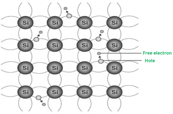
Formation and Behavior of Holes:
A large number of holes or vacant spaces in the covalent bond is created in the crystal with the addition of the trivalent impurity. A small or minute quantity of free electrons is also available in the conduction band. They are produced when thermal energy at room temperature is imparted to the germanium crystal, forming electron-hole pairs. However, the holes are more in number compared to the electrons in the conduction band. It is because of the predominance of holes over electrons that the material is called a p-type semiconductor.
The term “p” stands for positive material, reflecting the surplus of positive charge carriers (holes) in the material.
Difference Between Intrinsic and Extrinsic Semiconductors
| Intrinsic Semiconductor | Extrinsic Semiconductor |
|---|---|
| Semiconductor in its purest form. | Semiconductor doped with impurities. |
| It has low conductivity. | It has higher conductivity than intrinsic semiconductor. |
| The band gap between the conduction and valence band is quite narrow. | The energy gap is greater than that of an intrinsic semiconductor. |
| The Fermi level is typically found in the middle of the forbidden energy gap. | The position of the Fermi level depends on the type and concentration of impurities in the extrinsic semiconductor. |
| Electrical conductivity is determined mainly by temperature. | Electrical conductivity is affected by temperature and the concentration of impurity doping. |
| Pure Silicon and Germanium crystalline forms are examples. | Impurities such as arsenic (As), antimony (Sb), phosphorus (P), indium (In), bismuth (Bi), aluminum (Al), and others are doped into Silicon and Germanium crystals. |
Current Conduction in Semiconductor
Current conduction in semiconductors involves the movement of charge carriers, either electrons or holes, which are responsible for carrying electrical current through the material. This process is essential for the functioning of semiconductor devices like transistors, diodes, and integrated circuits.
Charge Carriers
In semiconductors, charge carriers are electrons and holes.
- Electrons: Negatively charged, they move from the negative terminal to the positive terminal when a voltage is applied.
- Holes: Essentially positive charges, they move from the positive terminal to the negative terminal.
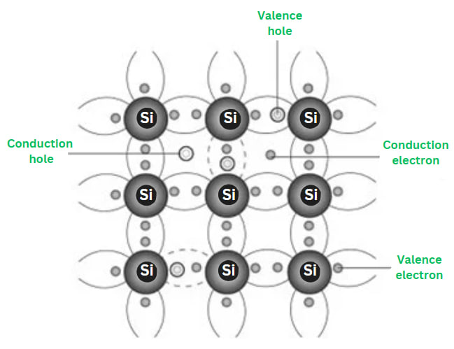
Conduction Through n-Type Semiconductor
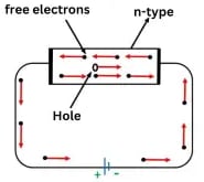
In an n-type semiconductor, a large number of free electrons are available in the conduction band, which are donated by the impurity atoms. The figure above illustrates the conduction process of an n-type semiconductor:
- When a potential difference is applied across this type of semiconductor, the free electrons move toward the positive terminal, thereby carrying an electric current.
- Since the current flow through the crystal consists of free electrons, which are carriers of negative charge, this type of conductivity is known as negative or n-type conductivity.
Electron-hole pairs are formed at room temperature. These holes, present in small quantities in the valence band, also contribute to the current, although minimally. For practical purposes, this contribution is often neglected.
Conduction Through p-Type Semiconductor
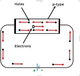
In a p-type semiconductor, a large number of holes are created by the trivalent impurity. When a potential difference is applied across this type of semiconductor, as shown in the figure above:
- The holes in the valence band move toward the negative terminal.
- The current flow through the crystal occurs via holes, carriers of positive charge, and this type of conductivity is known as positive or p-type conductivity.
- In p-type semiconductors, valence electrons move from one covalent bond to another.
The conductivity of an n-type semiconductor is nearly double that of a p-type semiconductor because the electrons in the conduction band of the n-type semiconductor are much more mobile than the holes in the valence band of a p-type semiconductor.
The mobility of holes is lower, as they are more strongly bound to the nucleus.
Even at room temperature, electron-hole pairs are formed. In p-type semiconductors, these free electrons, although present in minute quantities, also contribute to the current.
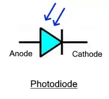
Photodiode
Photodiode is a type of semiconductor device used in electronics for detecting light or converting light energy into electrical signals. It operates based on the principle of the photovoltaic effect, where the absorption of photons (light particles) generates electron-hole pairs in a semiconductor material, creating an electric current. A photodiode is one type of light detector, used to convert the light into current or voltage based on the mode of operation of the device. It comprises optical filters, built-in lenses, and also surface areas. These diodes have a slow response time when the surface area of the photodiode increases. Photodiodes are similar to regular semiconductor diodes, but they may be either visible to let light reach the delicate part of the device. Several diodes intended for use specifically as a photodiode will also use a PIN junction rather than the usual PN junction.
Construction of Photodiode
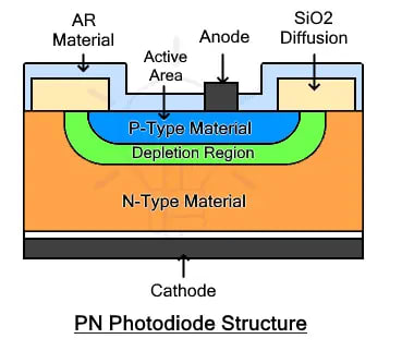
The construction of a photodiode involves the use of both P-type and N-type semiconductors to form a p-n junction. A typical photodiode is made from two layers of P-type and N-type semiconductor joined together to form a PN junction. As it is a light sensor, the junction is exposed to light rays by covering it with glass or an optical lens. The lens increases the surface area to collect more light and increase its intensity. The remaining portion of the photodiode is covered in a black layer or metalized.
- The given figure shows the cross-sectional structure of a typical PN photodiode.
- It is made from the joining of two layers P and N. The P-type material is lightly doped while the N-type material is heavily doped.
- The joining of these two layers forms a region due to the movement of (+) ions from P-type material and the movement of (-) ions from N-type material.
- This region is free of any charge carriers. However, there is an electric field across this depletion region.
- This electric field is responsible for the flow of current in only one direction when an electron-hole pair is generated.
- It is why photodiodes are reverse biased or not biased at all.
- Forward biasing may damage the photodiode permanently. The P+ active region is covered with an anti-reflective AR layer or glass while the remaining body is metalized or painted black. Metal contacts are used for cathode and anode.
Working of a Photodiode
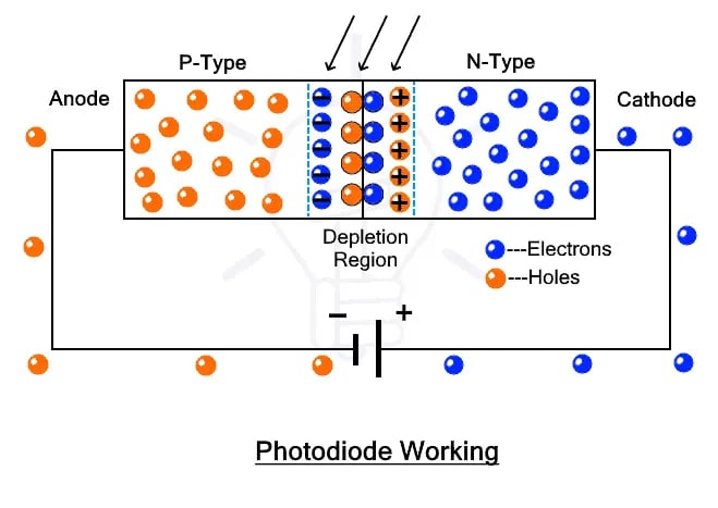
The working principle of a photodiode is, when a photon of ample energy strikes the diode, it creates a couple of an electron-hole. This mechanism is also called the inner photoelectric effect. If the absorption occurs in the depletion region junction, then the carriers are removed from the junction by the inbuilt electric field of the depletion region.
Therefore, holes in the region move toward the anode, and electrons move toward the cathode, and a photocurrent will be generated. The entire current through the diode is the sum of the absence of light and the photocurrent. So the absent current must be reduced to maximize the sensitivity of the device.
Modes of Operation
The operating modes of the photodiode include three modes, namely Photovoltaic mode, Photoconductive mode, and avalanche diode mode.
Photovoltaic Mode
This mode is also known as zero-bias mode, in which a voltage is produced by the illuminated photodiode. It gives a very small dynamic range and nonlinear necessity of the voltage formed.
Photoconductive Mode
The photodiode used in this photoconductive mode is more usually reverse biased. The reverse voltage application will increase the depletion layer's width, which in turn decreases the response time and the junction capacitance. This mode is too fast and displays electronic noise.
Avalanche Diode Mode
Avalanche diodes operate in a high reverse bias condition, which permits the multiplication of an avalanche breakdown to each photo-produced electron-hole pair. This outcome is an internal gain in the photodiode, which slowly increases the device response.
Phototransistors
A phototransistor is a type of semiconductor device that operates similarly to a regular transistor but is sensitive to light. It is designed to convert light energy into electrical signals, making it useful in various applications such as light detection and optical communication. A phototransistor is an electronic switching and current amplification component that relies on exposure to light to operate. When light falls on the junction, reverse current flows, which is proportional to the luminance. Phototransistors are used extensively to detect light pulses and convert them into digital electrical signals. They are operated by light rather than electric current. Providing a large amount of gain at low cost, these phototransistors might be used in numerous applications.
Symbol of Photo Transistor:
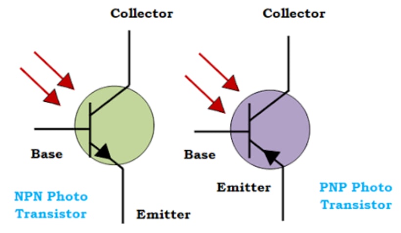
The symbol of Photo Transistor is similar to the transistor. The arrows shows the light incident on the base terminal.
Construction of Phototransistor
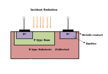
A phototransistor is is nothing but an ordinary bipolar transistor with its base region exposed to light. It is available in both P-N-P and N-P-N types and can be configured in various ways, such as common emitter, common collector, and common base. However, the common emitter configuration is the most commonly used. It can also operate with an open base. Compared to a conventional transistor, a phototransistor has larger base and collector areas.
Initially, phototransistors were made from a single semiconductor material like silicon or germanium. However, modern phototransistors are fabricated from materials such as gallium and arsenide to achieve higher efficiency. Finally, the phototransistor is enclosed in a metallic case with a lens placed on top to absorb incident radiation.
Working of Phototransistor
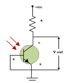
From the circuit above, it is evident that the base is not connected to any external bias; only light is incident on the base terminal. The collector terminal is connected to the positive side of the external supply, and the output is taken from the emitter terminal.
A phototransistor activates when light strikes the base terminal. The light triggers the phototransistor by creating hole-electron pairs and allowing current flow across the emitter and collector. As the current increases, it becomes concentrated and is converted into voltage. Generally, a phototransistor does not include a base connection. The base terminal is disconnected, as the light enables the flow of current throughout the phototransistor.
When no light is incident on the base terminal, only a small leakage current, known as dark current, flows. When light is incident on the base-collector junction, a base current is generated, which is proportional to the intensity of the incident light.
Types of Phototransistors
Phototransistors are classified into two types, namely BJT and FET.
BJT Phototransistor
In the absence of light, BJT phototransistor allows leakage among collectors and emitters of 100 nA or lower. Once this transistor is exposed to the beam, it performs up to 50mA. This distinguishes it from a photodiode, which cannot allow as much current.
FET phototransistor
This kind of phototransistor includes two terminals that connect inside through its collector and emitter or source and drain within FET. The transistor's base terminal reacts to light and controls the current flow among the terminals.
Difference between Photodiode and Phototransistor
| Photodiode | Phototransistor |
|---|---|
| The photodiode is a PN-junction diode used to generate electric current when a photon of light strikes its surface. | The phototransistor is a light-sensitive transistor that converts the energy of light into electrical energy. |
| It is less sensitive. | It is more sensitive. |
| The output response of the photodiode is fast. | The output response of the phototransistor is low. |
| It produces current. | It produces voltage and current. |
| It is used in solar power generation, detecting UV or IR rays, and also for light measurement, etc. | It is used in compact disc players, smoke detectors, lasers, invisible light receivers, etc. |
| It is more reactive to incident light. | It is less reactive. |
| The photodiode has lower dark current. | The phototransistor has higher dark current. |
| Both forward and reverse biasing can be used. | Only forward biasing is used. |
| The linear response range of the photodiode is much wider. | The linear response range of the phototransistor is narrower. |
| The photodiode is used for battery-powered devices that consume less power. | The phototransistor is used as a solid-state switch, unlike a photodiode. |
LED (Light Emitting Diode)

LED stands for Light Emitting Diode. It's a semiconductor device that emits light when an electric current passes through it. LEDs are widely used in electronics due to their energy efficiency, durability, and versatility.
The LED symbol is similar to a diode symbol except for two small arrows that specify the emission of light; thus, it is called an LED (light-emitting diode). The LED includes two terminals, namely the anode (+) and the cathode (-).
Construction
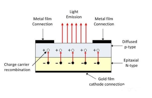
In an LED, the recombination of charge carriers occurs in the P-type material, which forms the surface of the LED. To achieve maximum light emission, the anode is positioned at the junction where the P-type and N-type materials meet. The cathode, typically made of a gold film, is usually located at the bottom of the N-region. This gold layer on the cathode helps reflect light back towards the surface.
Gallium arsenide phosphide is used in the manufacturing of LEDs that emit red or yellow light. LEDs are also available in green, yellow, amber, and red colors.
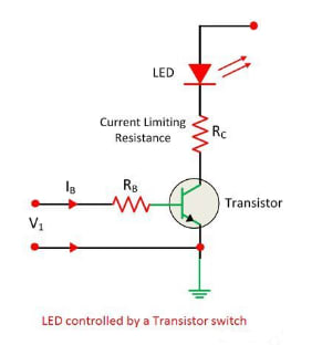
A simple transistor can be used to turn an LED on or off, as illustrated in the figure above. When the base current flows through the transistor, it allows the transistor to conduct heavily. The resistance limits the current flowing through the LED.
Working of LED
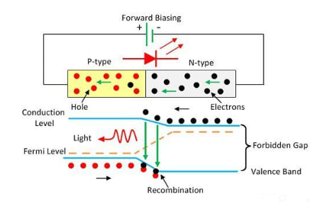
The operation of an LED is based on quantum theory. According to quantum theory, when electrons transition from higher energy levels to lower energy levels, they release energy in the form of photons. The energy of these photons corresponds to the energy gap between the higher and lower energy levels.
The LED is connected in a forward bias, allowing current to flow in the forward direction. This current flow is due to the movement of electrons in the opposite direction. During recombination, electrons transition from the conduction band to the valence band, emitting electromagnetic energy in the form of photons. The energy of these photons matches the energy gap between the valence and conduction bands.
Advantages of LED
- Size and Display Flexibility: LEDs are smaller in size and can be stacked together to form numeric and alphanumeric displays in high-density matrices.
- Temperature Range: LEDs operate over a wide temperature range, typically from 0° to 70°C. They are also durable and can withstand shocks and variations.
- Switching Speed: The on/off or switching time of LEDs is less than 1 nanosecond, making them suitable for dynamic operations.
- Economical and Reliable: LEDs are cost-effective and offer a high degree of reliability. They are manufactured using the same technology as transistors.
Disadvantages of LED
- Power Consumption and Cost: LEDs consume more power compared to LCDs, and their initial cost is higher.
- Limited for Large Displays: LEDs are not typically used for creating large displays.
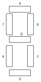
7-segment Display
A seven-segment display is a common type of electronic display device used to represent numerical digits and some alphanumeric characters. It consists of seven individual LED segments arranged in a specific pattern to form each digit from 0 to 9, plus additional segments for displaying letters A to F (in hexadecimal notation).
Working of a seven-segment display
The number 8 is displayed when power is given to all the segments, and if you disconnect the power for the segment 'g', then it displays the number 0. In a seven-segment display, power (or voltage) can be applied to different pins simultaneously, allowing for combinations to display numerical digits from 0 to 9. Since seven-segment displays cannot form alphabets like X and Z, they cannot be used for displaying the alphabet and are only suitable for displaying decimal numerical magnitudes. However, seven-segment displays can form alphabets A, B, C, D, E, and F, so they can also be used for representing letters.
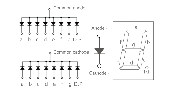
Each display unit usually has a dot point (DP). The display point could be located either towards the left or towards the right of the display pattern. This type of pattern can be used to display numerals from 0 to 9 and letters from A to F, representing hexadecimal digits.
Truth Table
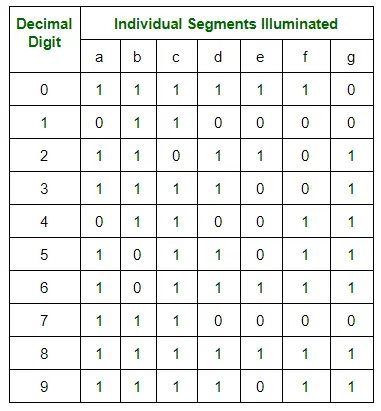
- Boolean expressions for each decimal digit that require respective light-emitting diodes (LEDs) to be ON or OFF.
- The number of segments used by digits 0, 1, 2, 3, 4, 5, 6, 7, 8, and 9 are 6, 2, 5, 5, 4, 5, 6, 3, 7, and 6 respectively.
- Seven-segment displays must be controlled by other external devices, where different types of microcontrollers are useful for communicating with these external devices, like switches, keypads, and memory.
Advantages & Disadvantages
Advantages
Clear and Easy to Read: Shows numbers and some letters clearly.
Cost-Effective: Affordable to manufacture and use.
Low Power Consumption: Saves energy, ideal for battery-powered devices.
Long Lifespan: Lasts a long time, reducing replacements.
Wide Voltage Range: Works with different power supplies.
Disadvantages
Limited Display Options: Can only show numbers and a few letters.
Limited Information: Can't display complex graphics or text.
Limited Color: Usually monochromatic, limited color options.
Segmented Appearance: Not aesthetically pleasing for some applications.
Complexity for Decimals: Challenging to display decimal points accurately.
Basic Electronics Engineering
Basic Electronics Engineering HPTU BTech CSE Syllabus
Semiconductor Diodes
p- n junction diode , Depletion layer , Energy diagrams of p-n junction and depletion region , Biasing of diode and V-I Characteristics; Rectifiers - half- wave , full- wave and bridge rectifiers; Filters - L , C , LC and π filters ; Zener diode , V-I Characteristics and Zener diode as voltage regulator.