Introduction
Nanoscience and nanotechnology are broad, interdisciplinary fields that have grown rapidly worldwide in recent years. Nanomaterials serve as the foundation of both nanoscience and nanotechnology. Today, key areas of research and development include energy, environmental science, water purification, and pharmaceuticals.
Nanomaterials have a wide range of applications, such as energy storage devices (e.g., fuel cells), defense systems for threat detection, drug delivery mechanisms, and water purification technologies. The industrial revolution significantly enhanced the quality of life, and many of today’s technologies—such as high-speed personal computers and mobile communication—would not have been possible without advancements in nanoscience and nanotechnology.
Nanoscience and Nanotechnology refers to the science and technology that deal with particles sized between 1 and 100 nanometers (nm).
Classification of Nanomaterials by Dimensions
Nanomaterials are classified based on the dimensional reduction of materials into three groups.
| S. No. | Reduction in size in different coordinates | Size | Examples |
|---|---|---|---|
| 1. | 3-dimensions | < 100 nm | Nanoparticles, quantum dots |
| 2. | 2-dimensions | < 100 nm | Nanotubes, nanowires, nanofibers |
| 3. | 1-dimension | < 100 nm | Thin films, coatings |
Classification Based on Pore Dimensions
Nanoporous materials can also be classified by the diameter of their pores. This parameter is crucial for applications involving adsorption and diffusion. The prefix "nano-" typically implies a size between 1 and 100 nm, within which material properties undergo significant changes. Pore diameter affects the types of molecules that can diffuse through the material and their interaction with the pore walls.
According to IUPAC, nanoporous materials are classified as follows:
-
Microporous materials
These have pore diameters less than 2 nm. They can accommodate only small molecules like gases and exhibit slow diffusion but strong interaction.
Examples: Na-Y, natural clay materials -
Mesoporous materials
With pore sizes between 2–50 nm, these can host larger molecules such as aromatic compounds. They are used as nano-reactors or in adsorption systems.
Examples: MCM-41, MCM-48, SBA-15, mesoporous carbon materials -
Macroporous materials (d > 50 nm)
These can accommodate very large molecules. Here, molecule-molecule interactions dominate. They are used for storing functional molecules or as scaffolds and sensing materials.
Examples: Carbon microtubes, porous gels, porous glasses
Properties of Nanomaterials
Nanomaterials exhibit significant changes in the following properties due to dimensional reduction:
Chemical Properties
-
Higher surface area
-
Greater number of surface-accessible atoms
-
Enhanced catalytic activity
-
Tunable surface properties based on shape, size, and composition. These features lead to increased rate, selectivity, and efficiency in chemical reactions.

Thermal Properties
- Melting point decreases as particle size decreases due to the increased proportion of surface atoms.
- Surface atoms are less tightly bonded and have more freedom to move.

Electronic Properties
- In bulk materials, electrons are free to move.
- At the nanoscale, quantum effects dominate.
- 0D nanomaterials: Electrons confined in all three dimensions
- 1D nanomaterials: Electrons confined in two dimensions
- Result: Discrete energy levels replace continuous energy bands, leading to behavior like semiconductors or insulators.
Optical Properties
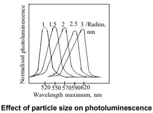
- Quantum confinement allows tuning of visible light emission by changing nanoparticle size.
- Reduction in size causes a blue shift in emission.
Magnetic Properties
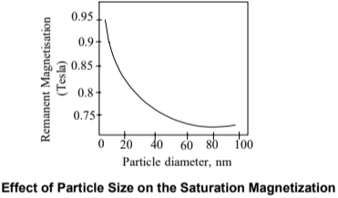
- Magnetic behavior is size-dependent.
- Below 20 nm, saturation magnetization increases significantly.
- This helps in designing better magnetic materials.
The catalytic and optical properties of nanomaterials differ significantly from those of bulk materials due to their extremely small size and unique structural characteristics. One major factor is the high surface area to volume ratio in nanomaterials, which means a much larger proportion of atoms are exposed on the surface. This leads to a significant increase in active sites available for chemical reactions, thereby enhancing their catalytic efficiency. Additionally, nanomaterials exhibit quantum size effects, where the confinement of electrons at the nanoscale alters their energy levels. This quantum confinement leads to size-dependent optical properties, meaning nanomaterials can absorb and emit light differently compared to their bulk counterparts. The electronic structure of nanomaterials is also modified at such scales, impacting how they interact with light and chemicals. Furthermore, certain metal nanoparticles, like gold or silver, show surface plasmon resonance—a phenomenon where electrons on the surface oscillate collectively in response to light, resulting in distinctive optical behaviors such as vivid colors. These combined factors explain why nanomaterials often have enhanced catalytic activity and unique optical properties not seen in bulk materials.
Graphene
Graphene, a single-atom-thick sheet of carbon atoms arranged in a hexagonal lattice, plays a pivotal role in chemistry due to its unique properties and potential for a wide range of applications. As a two-dimensional material, it exhibits exceptional strength, flexibility, and conductivity, making it a major focus of research in materials science, electronics, and energy storage.
Key Aspects of Graphene in Chemistry
1. Structure and Bonding
Graphene is composed of a single layer of carbon atoms bonded in a hexagonal lattice through strong covalent bonds. These bonds are responsible for its high melting point and remarkable mechanical strength.
2. Chemical Reactivity
Due to its two-dimensional structure, every atom in graphene is exposed and can participate in chemical reactions from both sides. Atoms located at the edges are especially reactive.
3. Functionalization
Graphene can be chemically modified by attaching atoms or molecules to its surface—a process known as functionalization. This allows tailoring its properties for specific applications.
4. Applications in Materials Science
Graphene’s high strength, flexibility, and surface area make it ideal for reinforcing composite materials, significantly enhancing their mechanical properties.
5. Applications in Electronics
Its superior electrical conductivity and transparency make graphene an excellent material for flexible electronics, touchscreens, and transistors.
6. Applications in Energy Storage
Due to its conductivity and large surface area, graphene is promising for use in supercapacitors and as an electrode material in batteries.
7. Applications in Chemistry
Graphene serves as a catalyst support, adsorbent, and reactive component in various chemical processes, expanding its usefulness in chemical research and industry.
Composition and Chemistry of Graphene Materials
Graphene is the thinnest known material in its class. It exhibits remarkable quantum effects, thermal conductivity, and mechanical properties, such as a high Young’s modulus (~1 TPa) and intrinsic strength (~130 GPa). It shows an ambipolar electric field effect with gate voltage and surpasses even diamond in terms of strength among carbon-based materials.
Graphene itself is chemically inert in many scenarios. However, its derivatives—such as graphene oxide (GO), reduced graphene oxide (rGO), and functionalized GO (fGO)—possess enhanced chemical activity and can be employed in a wide array of biomedical and engineering applications. The synthesis of graphene typically involves multiple sequential steps, such as micromechanical cleavage, anodic bonding, photo-exfoliation, liquid phase exfoliation, and silicon carbide processing.
Preparation Methods
Pure graphene is rarely used in research due to its limited yield from most synthesis processes. Instead, its derivatives like GO, rGO, and fGO are more widely used as they share similar properties and are easier to obtain.
Combination of Materials
Several scalable methods exist for synthesizing graphene, including mechanical exfoliation, chemical vapor deposition (CVD), liquid-phase reduction of GO, and epitaxial growth. These techniques fall under "top-down" or "bottom-up" approaches. Among them, CVD and mechanical stripping are commonly used. Since pure graphene does not readily react with oxygen, alternative methods are used to produce graphene oxide.
Liquid-Phase Exfoliation
The first successful synthesis of graphene oxide was performed by Brodie, who used a mixture of KClO₃ and HNO₃ vapors with graphite. While effective, the reaction is highly exothermic and can become hazardous. Carbon nanotubes were later introduced to moderate temperature, as they are stable in nitric acid and act as insulators. However, this method also led to the generation of harmful gases such as NO₂ and N₂O₄ at temperatures above 200°C. To control this, boron rods—commonly used in nuclear reactors—were incorporated to absorb excess energy and reduce gas emissions.
Chemical Vapor Deposition (CVD)
Small-scale techniques like mechanical exfoliation, CVD, and epitaxial growth have become standard. A variation involves transferring graphene grown on copper foils. Supercritical fluids can help control nanoparticle formation in graphene and its derivatives; however, their high cost and complex maintenance limit large-scale adoption. Further research is warranted in this area.
Synthesis of GO and rGO
When graphene is oxidized, it forms graphene oxide (GO), which can be further reduced to produce reduced graphene oxide (rGO). This material exhibits improved electrical properties, including high conductivity. Despite having similar chemical compositions, rGO exists in various forms and structures.
In bulk production, GO is immersed in a reducing agent under specific time and temperature conditions. This removes oxygen-containing functional groups such as -COOH and -OH.
Temperature Effect on GO Reduction
Thermal reduction is highly effective for producing quality rGO powders. GO is typically heated to temperatures around 1000 °C, causing oxygen and water molecules to be released.
UV Reduction:
GO can also be reduced using UV light, especially when dispersed in a solvent. This enhances UV absorption and facilitates reduction. Guo et al. proposed electrochemical reduction using a three-electrode system for GO suspensions. Strong π-π interactions and ionic interactions improve the final product’s properties. Although chemical and electrochemical reductions are viable, thermal reduction remains the most efficient, especially for powder forms. However, it is unsuitable for preserving thin films of GO.
Electrical Properties of Graphene-Based Materials
Most polymers are naturally insulating, but adding conductive fillers—such as graphene nanoplatelets (GNPs), carbon nanotubes (CNTs), or expanded graphite (EG)—can transform them into conductors. The percolation theory explains this transition: at low filler concentrations, the composite remains insulating, but beyond a certain threshold (percolation threshold), conductivity increases dramatically due to the formation of continuous conductive networks.
This threshold is influenced by the orientation and dispersion of nanofillers. For instance, Stankovich et al. reported a percolation threshold of 0.1 vol% in graphene-polystyrene composites, with conductivity increasing from 0.1 to 1 S/m as the graphene volume rose from 1 to 2.5 vol%. Graphene’s high aspect ratio and uniform dispersion were credited for this improvement.
The lowest reported percolation threshold for graphene-reinforced composites is around 0.07 vol%, while for CNT-reinforced HDPE composites, it is about 0.15 vol%. Xue Wang’s team achieved conductivity as high as 27 S/m using in-situ polymerization with high levels of polypyrrole doping.
Applications of Graphene and Its Derivatives
- Graphene boosts catalyst performance as a high-surface-area support.
- Doped graphene acts as a metal-free catalyst for various chemical reactions.
- Graphene enhances photocatalysis by improving charge separation.
- Graphene enables highly sensitive electrochemical sensors for diverse analytes.
- Graphene facilitates rapid and sensitive detection of various gases.
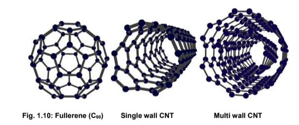
Fullerenes
Fullerenes are a unique class of carbon allotropes characterized by their closed, cage-like structures, which are typically spherical or cylindrical. Composed entirely of carbon atoms connected by single and double bonds, they form fused ring systems resembling spheres or tubes. The most well-known example is buckminsterfullerene (C₆₀), which resembles a soccer ball due to its highly symmetrical structure.
Key Aspects of Fullerenes in Chemistry
Structure
Fullerenes are formed by carbon atoms arranged in a closed, cage-like structure made of fused pentagonal and hexagonal rings. For instance, C₆₀ consists of 20 hexagons and 12 pentagons arranged in a truncated icosahedron.
Types
Fullerenes can take various forms, including:
- Spherical fullerenes (buckyballs)
- Cylindrical structures (carbon nanotubes)
- Hybrid forms and other structural variations
Properties
Due to their unique structure, fullerenes display:
- High thermal and chemical stability
- Excellent electron-accepting capabilities
- Exceptional mechanical strength
Synthesis Methods
Fullerenes are commonly synthesized using methods like:
- Laser ablation
- Electric arc discharge
These processes involve vaporizing carbon in an inert atmosphere to form fullerene molecules.
Classification of Fullerenes
Fullerenes are broadly categorized into two primary families:
- Closed-sphere fullerenes (buckyballs)
- Open-ended cylindrical structures (carbon nanotubes)
1. Spherical Fullerenes (Buckyballs)
C₆₀ (Buckminsterfullerene): The most iconic fullerene, consisting of 60 carbon atoms in a truncated icosahedron. Its structure closely resembles a soccer ball.
-
Higher Fullerenes:
Variants such as C₇₀, C₇₆, C₇₈, and C₈₄ possess larger carbon frameworks with different geometric arrangements. -
Heterofullerenes:
Carbon atoms in the cage may be substituted with heteroatoms like nitrogen or boron, altering electronic and chemical properties. -
Endohedral Fullerenes:
Atoms, ions, or small clusters are encapsulated inside the carbon cage, significantly modifying electronic and magnetic behavior—ideal for applications in medicine, catalysis, and electronics.
2. Carbon Nanotubes (CNTs)
-
Single-Walled Nanotubes (SWNTs): Formed by rolling a single graphene sheet into a seamless cylinder.
-
Multi-Walled Nanotubes (MWNTs): Consist of multiple concentric cylinders of graphene, nested within one another.
Applications of Fullerenes
Fullerenes are employed in various industries due to their exceptional properties:
-
Electrical Conductors: Some fullerene structures are excellent electron acceptors and can enhance conductivity.
-
Gas Absorption: Their cage-like structures make them suitable for gas storage and separation.
-
Lubricants: Their spherical shape allows them to reduce friction at the molecular level.
-
Cosmetics: Used in skincare for their antioxidant properties and molecular stability.
-
Biomedical Applications: Certain fullerenes and carbon nanotubes are explored for drug delivery, imaging, and cancer treatment.
-
Advanced Textiles: Carbon nanotube-based fibers and fabrics exhibit enhanced strength, flexibility, and conductivity.
Carbon Nanotubes
Carbon is the lightest element in Group IV of the periodic table and exhibits unique chemical versatility due to its ability to form strong covalent bonds with itself and with other light elements. This characteristic gives rise to the vast field of organic chemistry, which forms the basis of biochemistry and the foundation of life itself. Carbon exists in several allotropic forms, including diamond and graphite, each exhibiting distinct structural and physical properties.
In 1991, Sumio Iijima made a groundbreaking discovery by capturing transmission electron microscope images of elongated, concentric, layered microtubules composed entirely of carbon atoms. These structures were later identified as multi-walled carbon nanotubes (MWCNTs). This discovery sparked a surge in research into one of the most intriguing nanostructures of the 20th century: carbon nanotubes (CNTs). CNTs have since become a focal point in materials science, chemistry, and physics due to their exceptional properties.
Two years after Iijima's discovery, researchers identified another variation—single-walled carbon nanotubes (SWCNTs)—which consist of a single cylindrical layer of carbon atoms. Both types of nanotubes belong to the broader class of fullerenes, a family of carbon-based nanostructures characterized by their closed-cage architectures.
Fullerenes and Their Significance
Fullerenes were first discovered in 1985 by Harold Kroto, Robert Curl, and Richard Smalley. These unique carbon allotropes were named in honor of architect Buckminster Fuller, whose geodesic dome designs resembled the highly symmetric, hollow shapes of the molecules. The most well-known fullerene, C₆₀, resembles a soccer ball, consisting of 12 pentagons and 20 hexagons. In these molecules, all carbon atoms are sp² hybridized, similar to graphite, but arranged in a spherical rather than planar configuration.
Fullerenes and their tubular counterparts—carbon nanotubes—are considered the third major allotrope of carbon, following diamond and graphite. While fullerenes appear as spheroidal molecules (commonly called "buckyballs"), carbon nanotubes are essentially long, cylindrical fullerenes with nanometer-scale diameters and lengths that can range from micrometers to centimeters.
Due to their remarkable mechanical strength, electrical conductivity, thermal stability, and chemical tunability, carbon nanotubes have emerged as one of the most promising materials in nanotechnology. Their potential spans a wide range of applications, from nanoelectronics and energy storage to drug delivery and advanced composite materials.
Types of Carbon Nanotubes
Carbon nanotubes (CNTs) are cylindrical nanostructures composed entirely of carbon atoms, with diameters on the nanometer scale. Their structure can be visualized as a graphene sheet— a single atomic layer of carbon atoms arranged in a hexagonal lattice—rolled into a seamless cylinder. Depending on their geometry, helicity, number of walls, and dimensions, CNTs exhibit diverse structures and unique properties.
1. Single-Walled Carbon Nanotubes (SWCNTs):
SWCNTs consist of a single layer of graphene rolled into a cylindrical form, typically capped at the ends. These nanotubes generally have diameters around 1 nm, but their lengths can be thousands of times longer. SWCNTs are known for their flexibility and can be twisted, bent, or even looped without breaking. Despite their superior electrical and mechanical properties, they are more challenging to synthesize compared to MWCNTs.
2. Multi-Walled Carbon Nanotubes (MWCNTs):
MWCNTs consist of multiple concentric cylindrical layers of graphene. There are two models describing their structure:
- Russian Doll Model: Smaller nanotubes are nested within larger ones.
- Parchment Model: A single graphene sheet is rolled multiple times, resembling a scroll.
Double-walled CNTs (DWNTs) are the simplest form of MWCNTs. Their diameters typically range from 5 nm to 50 nm. MWCNTs offer greater tensile strength and enhanced chemical resistance, thanks to their outer walls protecting the inner tubes. While they are easier to produce, their structural complexity and imperfections make their properties harder to characterize.
Synthesis of Carbon Nanotubes
Several techniques are available for producing both single-walled and multi-walled carbon nanotubes (SWCNTs and MWCNTs), each with its own advantages and disadvantages. These methods can broadly be classified into two categories based on the temperature range involved: high-temperature and medium-temperature processes.
The three most important techniques for synthesizing high-quality CNTs are Laser Ablation, Arc Discharge, and Chemical Vapour Deposition (CVD). More recently, arc discharge in liquid media has emerged as a low-cost method capable of synthesizing various nano-carbon structures such as carbon onions, carbon nanohorns, and carbon nanotubes. This method is advantageous as it eliminates the need for expensive apparatus.
Electric Arc Discharge Method (Plasma Arcing)
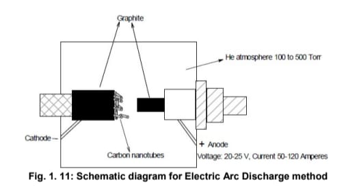
The electric arc discharge method is one of the most common techniques for fabricating carbon nanotubes. It involves an electrical breakdown of a gas, producing a plasma discharge that occurs in a gas-filled chamber between two graphite electrodes. The arc generates temperatures around 6000°C, sufficient to sublimate carbon from the graphite.
A schematic of the arc discharge setup is shown in Fig. 1.11. In this method:
- Two pure graphite electrodes (anode and cathode) are positioned 1–2 mm apart.
- A hole is drilled into the anode and filled with a mixture of metal catalyst powders (e.g., iron, cobalt, nickel, or yttrium) and graphite powder.
- The chamber is filled with an inert gas such as helium or argon, typically using a diffusion pump.
At high temperatures, carbon atoms sublimate from the anode, form a plasma, and then deposit on the cathode surface to form carbon nanotubes. The presence of metal catalysts promotes the formation of single-walled CNTs, whereas their absence favors multi-walled CNTs.
During the process, web-like structures form around the cooler parts of the electrodes, within which bundles of 10–100 SWCNTs are observed. This method typically yields about 25% pure CNTs, though efficiency has improved with the use of combined nickel-yttrium catalysts, enhancing both the quality and quantity of SWCNTs.
Electric Arc Discharge in Liquid Media
The traditional arc discharge method requires complex equipment, including gas handling systems, sealed reaction chambers, and multiple purification steps. In contrast, arc discharge in liquid media simplifies the process, providing more uniform and efficient CNT synthesis.
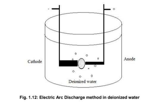
As illustrated in Fig. 1.12:
- Two graphite electrodes are placed 1–2 mm apart in an open vessel filled with deionized water or liquid nitrogen.
- The anode (6 mm diameter) has a 5 mm hole filled with a graphite and metal catalyst powder mixture. The cathode diameter ranges from 12–20 mm.
- Initially, the electrodes are in contact and connected to a DC power supply.
- Arc discharge is initiated by slowly separating the movable anode from the cathode, maintaining a 1 mm gap.
The resulting arc causes the carbon in the anode to sublimate and deposit as a crust on the cathode. The growth rate of CNTs is influenced by the applied voltage. A constant temperature of around 25°C is considered ideal for this method. NaCl solution has also been explored recently as a viable liquid medium for CNT synthesis.
Chemical Vapour Deposition (CVD)
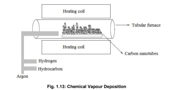
Chemical vapour deposition is a well-established technique for synthesizing various carbon materials, including CNTs. It involves the thermal decomposition of hydrocarbon vapors over a metal catalyst and is known for producing high yields of defect-free CNTs at relatively low temperatures.
As shown in Fig. 1.13, the process includes:
- Using a substrate like quartz or alumina, which is cleaned and prepared for catalyst deposition.
- Deposition of a metal catalyst (e.g., iron or nickel) on the substrate surface via thermal evaporation.
- Heating the substrate in a tubular furnace to a temperature between 600°C and 1200°C.
- Introducing hydrocarbon vapors (such as acetylene, ethylene, or carbon monoxide) into the furnace.
For liquid hydrocarbons (e.g., benzene, alcohol), they are vaporized by purging an inert gas through a heated flask. Solid precursors like camphor or naphthalene are placed directly in the low-temperature zone of the furnace, from where they sublimate and participate in the CNT growth.
At high temperatures, carbon dissociates from the hydrocarbon molecules, dissolves in the catalyst, and precipitates as CNTs on the catalyst surface as the system cools.
Growth Mechanisms in CVD
Two primary growth models explain how CNTs form:
-
Tip Growth Model (Top Carbon Diffusion):
Carbon decomposes on the exposed surface of the metal catalyst, dissolves into it, and diffuses through the particle before precipitating as nanotubes. The catalyst remains at the tip of the growing tube. -
Base Growth Model (Bottom Carbon Diffusion):
The catalyst stays anchored to the substrate. Carbon dissolves into it and precipitates above the catalyst, leading to nanotube growth from the base.
The type of nanotube formed depends on the catalyst particle size—SWCNTs form from smaller particles (a few nanometers), whereas MWCNTs form from larger ones.
Compared to arc discharge and laser ablation, CVD offers a more economical and scalable solution for CNT synthesis under ambient pressure and lower temperatures. Though arc and laser methods produce CNTs with superior crystallinity, the yield and purity of CNTs are higher in CVD, particularly for MWCNTs. Notably, CVD-grown SWCNTs can rival those produced by arc and laser methods in terms of quality.
CVD also excels in structural control and versatility. It supports the use of solid, liquid, or gaseous hydrocarbon precursors, accommodates various substrates, and enables growth of CNTs in diverse forms—powders, films, aligned or entangled structures, and architected nanotube arrays on patterned substrates. Additionally, it allows precise control over growth parameters, making it the most flexible technique for CNT production.
Properties of Carbon Nanotubes
Electrical Properties
The electrical properties of carbon nanotubes (CNTs) depend on the orientation of the hexagonal carbon rings along the tube’s axis. CNTs can be categorized based on the chiral vector (n, m), which determines how the graphene sheet is rolled. There are three main configurations: armchair, zigzag, and chiral.
- Armchair CNTs (where n = m) have hexagons oriented parallel to the tube axis. These behave like metals. When a voltage is applied between their ends, they exhibit excellent conductivity—surpassing even copper.
- Zigzag CNTs (where m = 0) have hexagons aligned in circular patterns around the tube.
- Chiral CNTs (where n ≠ m and m ≠ 0) exhibit a twisted pattern.
Zigzag and chiral CNTs generally behave like semiconductors, conducting electricity only when additional energy—such as light or an electric field—is applied to excite electrons.
The electronic properties of single-walled carbon nanotubes (SWCNTs) are defined by their diameter and helicity. A SWCNT results from wrapping a graphene sheet seamlessly along the roll-up vector (n, m). This vector determines the tube’s radius, chirality, and ultimately, its electronic structure.
The chiral vector is defined using two lattice vectors a₁ and a₂, which are not perpendicular but define the hexagonal structure of graphene. The pair (n, m) specifies how many steps along each direction are needed to roll the sheet into a nanotube:
- A (3, 0) CNT moves 3 units in the a₁ direction.
- A (3, 3) CNT moves 3 units each in the a₁ and a₂ directions.
The chiral angle (θ) lies between 0° and 30°:
- Armchair CNTs have θ = 30° and are always metallic.
- Zigzag CNTs have θ = 0° and are metallic only if (n − m) is a multiple of 3 (i.e., n − m = 3i, where i is an integer). Otherwise, they are semiconducting.
- Chiral CNTs fall between these two extremes (0° < θ < 30°).
Carbon nanotubes can carry nearly 1000 times more current than copper, making them exceptional conductors under appropriate conditions.
Mechanical Properties
Tensile strength describes how much force a material can withstand before breaking. CNTs are among the strongest known materials, characterized by high Young’s modulus and tensile strength.
Their extraordinary strength is due to:
- Strong sp² carbon-carbon covalent bonds.
- The fact that a CNT is a single molecule—free from grain boundaries and weak points common in polycrystalline materials like steel.
- Graphite’s in-plane modulus is ~1.06 TPa. CNTs show similar or higher stiffness:
- SWCNTs: Young’s modulus ranges from 0.32 to 1.47 TPa; tensile strength from 10 to 52 GPa.
- MWCNTs: Modulus ranges from 0.27 to 0.95 TPa; tensile strength from 11 to 63 GPa.
CNTs are lightweight, with a density between 1.3 and 1.4 g/cm³, about one-fourth that of steel.
They are also elastic. Studies using atomic force microscopes and transmission electron microscopes show CNTs can bend or compress without breaking their atomic bonds.
CNTs also exhibit excellent thermal conductivity—predicted to exceed that of silver by over ten times. Unlike metals (which conduct heat via electron movement), CNTs transfer heat through vibrational energy in their atomic bonds.
Vibrational Properties
Atoms in molecules and nanostructures undergo continuous vibrations. CNTs have two significant normal modes of vibration, governed by their symmetry:
- Ag mode: A radial "in-and-out" oscillation of the tube’s diameter.
- E2g mode: A distortion where the tube alternately squashes and expands, shifting between spherical and elliptical shapes.
The vibrational frequencies of these modes depend on the tube’s radius and are now used to estimate it experimentally.
Applications of Carbon Nanotubes
- Catalyst Supports: High surface area and chemical stability make CNTs excellent supports for catalysts.
- Hydrogen Storage: CNTs have potential in hydrogen storage for hydrogen-oxygen fuel cells.
- AFM Probe Tips: CNTs are ideal for manufacturing atomic force microscope (AFM) tips due to their high aspect ratio and stiffness.
- Drug Delivery: CNTs can act as drug carriers, capable of penetrating cell membranes and even nuclei.
- Actuators/Artificial Muscles: CNTs convert electrical energy into mechanical movement, useful in nano-actuators.
- Sensors: CNTs serve as sensing materials in pressure, thermal, chemical, gas, optical, and biological sensors.
- Field Emission: Their low turn-on voltage, high current density, and durability make CNTs excellent for field emission devices.
- Touch Screens: Thin CNT films (~10–20 nm) are transparent and conductive, useful in touch screens, OLEDs, and solar cells.
- Structural Applications: CNTs offer superior stiffness and strength for creating lightweight yet strong materials in construction and engineering.
- Aerospace Components: Their excellent fatigue strength over time makes CNTs suitable for aircraft and spacecraft components.
Nanowires
Nanowires are cylindrical solid structures with at least one dimension smaller than 100 nm and lengths extending up to several micrometers. When their diameter is comparable to the electron’s de Broglie wavelength in the direction perpendicular to their growth axis, nanowires behave as quantum mechanically one-dimensional structures.
This one-dimensional confinement of electrons alters the density of states and the allowed energy levels within nanowires. Quantum confinement also enables the observation of unique phenomena such as ballistic transport, Coulomb blockade, and phonon confinement. One particularly interesting feature of nanowires is the tunability of their bandgap, a crucial parameter for designing devices for specific applications. As the diameter of a nanowire decreases, the bandgap increases, allowing efficient visible light emission. Additionally, due to their high surface area-to-volume ratio, nanowire bandgaps are highly sensitive to surface chemistry. The nature of the surface passivant can either increase or decrease the bandgap accordingly.
A widely accepted method for growing nanowires through gas-phase reactions is the Vapour-Liquid-Solid (VLS) mechanism. For nanowire growth, the material to be deposited must be soluble in the catalyst nanoparticles. For instance, silicon nanowires are typically grown using gold nanoparticles, as silicon vapor is soluble in gold. Similarly, iron nanoparticles are used for growing gallium nitride nanowires, since both gallium and nitrogen reactants are soluble in iron.
Synthesis of Silicon Nanowires (Vapour-Liquid-Solid Mechanism)
The VLS mechanism was first proposed in 1964 to explain the growth of silicon whiskers from the gas phase in the presence of a liquid gold droplet on a silicon substrate. It is now widely used for synthesizing one-dimensional structures such as nanowires.
Direct crystal growth from the gas phase onto a solid surface is typically slow. The VLS mechanism overcomes this limitation by introducing a catalytic liquid alloy phase that rapidly absorbs vapor-phase reactants until supersaturation is achieved. Once supersaturation is reached, crystal growth proceeds from nucleated seeds at the liquid–solid interface. The physical characteristics of nanowires grown via this method depend, in a controllable way, on the size and properties of the liquid alloy catalyst.
The VLS process involves two main steps:
-
Step 1: The vapor-phase reactant (e.g., silane, SiH₄) diffuses into the gold liquid catalyst nanoparticles.
-
Step 2: Once supersaturation of silicon is reached in the liquid phase, it precipitates out as a solid, forming the nanowire.

Figure 1.5: Vapour–Liquid–Solid mechanism for the synthesis of silicon nanowires. The process begins by coating a substrate with gold nanoparticles, which are then heated in a furnace until they melt. Silane (SiH₄) is introduced into the chamber and vaporizes, forming silicon vapor. This vapor diffuses into the molten gold nanoparticles. When the silicon concentration reaches supersaturation, it begins to precipitate and grow into nanowires.
Criteria for an Effective Catalyst in VLS Mechanism:
- The catalyst must remain chemically inert with respect to the reaction products.
- It should exhibit low solid solubility in both the solid and liquid phases of the material being grown.
- It must form a liquid solution with the crystalline material at the nanowire growth temperature.
Applications of Nanowires
- Nanowires are used in electronic devices such as field-effect transistors, light-emitting diodes, biosensors, optical switches, solar cells, and photodetectors.
- They can replace traditional copper interconnects in computers and other electronics.
- Self-assembled nanowires offer high chemical tunability, making them ideal building blocks for nano-scale devices. This is particularly useful in communication systems through miniaturization of light sources, and in the advancement of nanotechnologies and biosensors.
- The Vapor–Liquid–Solid (VLS) process remains a widely applied and effective method for nanowire synthesis, typically using metal catalysts.
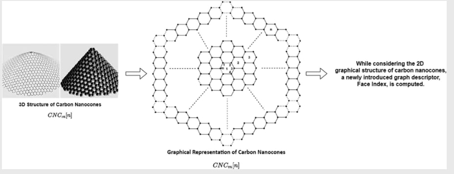
Nanocones
Nanocones, also known as carbon nanohorns (CNHs), are conical carbon nanostructures composed of sp²-hybridized carbon atoms that form closed cage-like geometries. They are notable for their high surface area, exceptional mechanical stability, and distinct electronic properties, making them valuable for a wide range of applications.
Key aspects of nanocones in chemistry:
Structure:
Nanocones typically consist of sp²-hybridized carbon atoms arranged into a conical shape, featuring a central pentagonal ring at the apex. This unique geometry contributes to their structural stability and electronic characteristics.
Synthesis:
They can be synthesized through various techniques, such as the decomposition of hydrocarbons using a plasma torch or by introducing defects into graphene sheets. These methods enable the controlled formation of the nanocone structure.
Properties:
Nanocones exhibit a high surface-to-volume ratio and surface area, along with superior mechanical stability compared to other one-dimensional nanomaterials like carbon nanotubes. These features enhance their performance in both structural and functional applications.
Applications:
Owing to their unique properties, nanocones find applications in multiple areas, including:
- Energy storage and conversion: Investigated for use in fuel cells, water splitting, and solar cells due to their favorable electrochemical behavior.
- Biosensors: Their closed-cage structure can be functionalized to detect specific biological molecules.
- Nanohybrid devices: Serve as components in advanced devices by combining with other nanomaterials.
- Gas storage and sensing: Suitable for storing and sensing various gases due to their porous and reactive surfaces.
- Catalysis: Their surfaces and electronic properties are being explored for catalyzing a range of chemical reactions.
Functionalization:
The surfaces of nanocones can be chemically modified with functional groups to enhance their dispersibility, enable bioconjugation, and tailor their properties for specific applications.
Example:
Carbon nanohorns (CNHs): A specific class of nanocones, CNHs have been extensively studied for their potential in energy storage, catalysis, and biosensing, attributed to their distinct conical structure and physicochemical characteristics.
Applications of nanomaterials
In modern life, the demand for materials with novel properties continues to grow, driving technological advancement. The emergence of nanomaterials has significantly accelerated discoveries across various scientific fields. Due to their exceptional electronic, optical, magnetic, thermal, and catalytic properties, nanomaterials have attracted widespread interest and are now employed in physics, chemistry, biology, medicine, materials science, and numerous interdisciplinary domains.
Nanomaterials are distinguished by their extremely small particle size and large surface area, which greatly enhance their interaction with surrounding environments. Their lack of point defects contributes to a mechanical strength that can be up to ten times greater than that of steel. These characteristics explain why even a small amount of nanomaterial can outperform much larger quantities of conventional materials.
Today, nanomaterials are used in a wide range of sectors, including:
- Production technologies
- Military engineering
- Nuclear power engineering
- Electronic equipment
- Surface protection of materials
- Medicine and biotechnology
Production Technologies:
- Nanomaterials are increasingly used in composites as multifunctional components.
- Adding nanopowders to steel and alloy production reduces porosity and enhances mechanical properties.
- Superplasticity in nanostructured aluminum and titanium alloys makes them ideal for manufacturing complex parts and for use as connecting layers in solid-state welding.
- Their large specific surface area makes nanopowders highly effective as catalysts in various chemical processes.
Military Engineering:
- Ultrafine powders are used in radar-absorbing coatings for stealth aircraft and in advanced explosives and incendiary devices.
- Carbon nanofibers are incorporated into specialized munitions like graphite bombs, designed to disrupt enemy power systems.
Nuclear Power Engineering:
Ultrafine powders have been integral to the early development of nuclear power, particularly in isotope separation of uranium. Advancements in nuclear energy are focused on using nanomaterials to reduce natural uranium consumption by increasing fuel burn-up efficiency. Research is ongoing into forming porous, coarse-grained structures in nuclear materials to enhance fission product retention.
Material Surface Protection:
For certain applications, high water- and oil-repellency is essential—such as in car windows, aircraft glass, ships, protective clothing, storage tanks, and building materials. Titanium dioxide nanoparticle coatings (20–50 nm) combined with polymer binders have been developed to significantly reduce surface wettability with water, oil, and alcohol-based solutions.
Medicine and Biotechnology:
Nanotechnology is applied in several key biomedical areas:
1. Targeted Drug Delivery:
In cancer therapy, nanoparticles help protect drugs from degradation, minimize adverse interactions, and increase selective absorption by tumor cells. They enhance pharmacokinetics, improve bioavailability, and can also deliver genetic material into cells.
2. Treatment and Prosthetics:
The mechanical and biocompatible properties of nanomaterials enable the development of durable implants and prosthetics that are safe for long-term use in the body.
3. Diagnostics:
Nanotechnology enhances imaging, characterization, and analysis of biological samples, providing high-resolution diagnostics. Magnetic nanoparticles—especially iron oxide coated with polymers—serve as biosensors. These coatings can be functionalized with biospecific ligands and shield the particles from adverse interactions with biological molecules. Other materials, such as nanotubes and metallic nanoparticles, are used in electrochemical sensors.
Electronic Equipment:
Carbon nanotubes have revolutionized electronics by offering alternatives to traditional transistors. They enable the development of flexible, transparent circuits due to their exceptional mechanical and optical properties. Their mobility and light-transmitting capability allow the creation of bendable electronics without performance loss.
Nanotechnology has also led to new hard disk designs. The 2007 Nobel Prize in Physics recognized the discovery of the giant magnetoresistance (GMR) effect, enabling the development of highly sensitive magnetic field sensors that allow near-atomic resolution in data reading.
Another promising application is in solar energy. Replacing traditional metal wires with nanowires in solar cells has been shown to increase energy absorption by up to fifteen times. Nanostructured materials improve efficiency and lower costs in photovoltaic devices.
Examples of Specific Nanomaterials and Their Uses:
- Silver nanoparticles: Known for antibacterial properties; used in surgical instruments, refrigerators, air purifiers, and more.
- Gold nanoparticles: Used in drug delivery, cancer detection, and catalytic synthesis of silicon nanowires.
- ZnO nanoparticles: Employed in UV emitters, piezoelectric devices, and chemical sensors.
- TiO₂ nanoparticles: Function as photocatalysts and are used in sunscreens for UV protection.
- ATO/ITO nanoparticles: Applied in car windows, LCDs, and solar cells.
- Nanoscale materials (nanoparticles, nanowires, nanofibers, nanotubes): Widely used in biosensing, biological separation, imaging, and cancer therapies. Their high surface-to-volume ratio, surface modifiability, solubility, and multifunctionality offer vast potential in biomedicine.
- These materials provide unique optical, magnetic, and biological properties that allow precise control of complex biological processes.
- Nanomaterials are also extensively used in water purification, wastewater treatment, environmental remediation, food packaging, and smart sensor technologies.
- In agriculture, they are used for crop enhancement and protection.
- Nanomaterials derived from metals, semiconductors, carbon, or polymers are also used as electrode modifiers to improve the performance of electrochemical biosensors.